Continue to Site

Welcome to EDAboard.com

Welcome to our site! EDAboard.com is an international Electronics Discussion Forum focused on EDA software, circuits, schematics, books, theory, papers, asic, pld, 8051, DSP, Network, RF, Analog Design, PCB, Service Manuals... and a whole lot more! To participate you need to register. Registration is free. Click here to register now.

frequency shift between simulation and measurements

Status
Not open for further replies.

inass57

Member level 2
Member level 2
Joined
Jan 18, 2018
Messages
48
Helped
1
Reputation
2
Reaction score
1
Trophy points
8
Activity points
431
hi guys!

I have designed an LNA working at 9.35GHz with ADS using cosimulation. here is its layout:
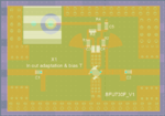
BFU730F.PNG

I have printed two of this LNA to compare to my simulation and i have a frequency shift, as shown in the picture below.
I have checked the substrate height, copper thickness but i have doubts about the permitivitty of the substrate (i'm using RO4003C) but i should mention that i didn't have those frequency shifts on my filters.

Any insight would be appreciated. thank you in advance.

mesure.PNG
 

It's the old saying, "In theory, there is no difference between theory and practice. In practice, there is."

Obviously, you didn't account for all the variables in your circuit - nobody does, because you don't know what you don't know. In your design, you should provide places to add additional caps, trim lines, etc.
 
  • Like
Reactions: FvM

    FvM

    Points: 2
    Helpful Answer Positive Rating
If you have VNA, plotting S11/S22 on a Smith Chart for measurement and simulation may be useful. I would try to tune dimensions until curves on a Smith Chart for simulation and measurement look similar.

Also I would try to build few calibration boards (50ohm line, stub, series capacitor, line with feeding line and radial stub), simulate then and measure them. Though you said filters are measured ok.

I would replace c1 and c2 with quarterwave coupled microstrip lines (0.2mm width / 0.2mm gap or thinner). In my opinion such DC blocks are more predictable.
 

I think the differences are coming from components' tolerances.A tuning is necessary because the frequency is pretty high..
Have you ever done a Monte Carlo Analysis ?? You'd better do it..
 

with ADS using cosimulation

What models have you used for C1 and C2?

For the transistor, usually some ground path is included in the measured data, so you might have added it a again when using that S2P file with EM co-simulation (S2P ground cascaded with EM modelled ground path). Check sensitivity of ground path inductance on results.
 

What models have you used for C1 and C2?

For C1 and C2 i used the a Murata capacitor and included its model on the simulation.

For the transistor, usually some ground path is included in the measured data, so you might have added it a again when using that S2P file with EM co-simulation (S2P ground cascaded with EM modelled ground path). Check sensitivity of ground path inductance on results.

I'm sorry i don't understand what you just said could you please explain it a little bit more or maybe guide me to some litterature.

- - - Updated - - -

I think the differences are coming from components' tolerances.A tuning is necessary because the frequency is pretty high..
Have you ever done a Monte Carlo Analysis ?? You'd better do it..

I was thinking about that but since the two LNAs i have tested gave the same response i'm a little bit skeptical about it.
 

For C1 and C2 i used the a Murata capacitor and included its model on the simulation.
What are their values ?? Tune them a bit, for instance use 0.1pF or 0.2pF lower values to shift the matching frequency to the rightif they are included in matching circuit.( few pF )
 
For C1 and C2 i used the a Murata capacitor and included its model on the simulation.

The models provided by Murata? I don't know how accurate these models are (possibly great), but more important: where the reference planes are (pad center? outer edge? ) and if they include some pad effects (not desirable if you include pads in EM simulation already).

You can check by moving the pin position on the pad, and check for a mistake in pad capacitance (if measured data used other substrate thickness, or measured data included pad effect and you add it again in EM) by adding a small positive/negative shunt C to model. Does it look closer to measurement then?

Modelithics have a library of substrate scalable models for different manufacturers, and what I like about their models is that it is very clearly defined where the references planes are, what is included etc.

I'm sorry i don't understand what you just said could you please explain it a little bit more or maybe guide me to some litterature.

The transistor model is based on measured data, and for measurement the transistor source is grounded. That ground path is then included in results. Now you use the S2P model and connect the ground of the S2P data to some place in layout. The path from that ground pin to PCB ground has inductance, and that is in series with the S2P ground path from measurement. This can create over-estimate of ground path inductance, because your S2P includes the measured ground path and in your EM model you add another ground path between S2P ground pin and PCB ground.
 
Last edited:
Capacitors are apparently 0603 size which is huge for 9 GHz range. If the used model includes the series inductance, it's unlikely to be valid for the unusual large pad distance in your design.
 
Capacitors are apparently 0603 size which is huge for 9 GHz range.

The size should be ok, it is reasonable compared to the line. But indeed, the model accuracy might be compromised. Are these just DC blocks or do they implement a specific impedance? What values and types are these caps?

Looking at the pin position on the edge, in line width the open stub, I suspect we might have an issue with ADS Momentum port width. That's an all time classic for this type of layout: when you place a pin on the edge, ADS places the EM port along the entire edge including the stub. This wrong port width then results in simulation error. More details and solution: https://muehlhaus.com/support/ads-application-notes/edge-area-pins

portwidth.PNG
 
The models provided by Murata? I don't know how accurate these models are (possibly great), but more important: where the reference planes are (pad center? outer edge? ) and if they include some pad effects (not desirable if you include pads in EM simulation already).

You can check by moving the pin position on the pad, and check for a mistake in pad capacitance (if measured data used other substrate thickness, or measured data included pad effect and you add it again in EM) by adding a small positive/negative shunt C to model. Does it look closer to measurement then?

Modelithics have a library of substrate scalable models for different manufacturers, and what I like about their models is that it is very clearly defined where the references planes are, what is included etc.

I actually don't include the pads in the EM simulation just the lines. the SMT are just drawn but not simulated.
In this link they explain how they got their model but it doesn't mention if it's at the center pad or the outer edge.


The transistor model is based on measured data, and for measurement the transistor source is grounded. That ground path is then included in results. Now you use the S2P model and connect the ground of the S2P data to some place in layout. The path from that ground pin to PCB ground has inductance, and that is in series with the S2P ground path from measurement. This can create over-estimate of ground path inductance, because your S2P includes the measured ground path and in your EM model you add another ground path between S2P ground pin and PCB ground.

the model i used on ADS for the transistor is a MEXTram Model. do you think there might be the same problem even if it's a diffrent model? i'm not sur how those models are made but from my simulations they are more accurate.

- - - Updated - - -

The size should be ok, it is reasonable compared to the line. But indeed, the model accuracy might be compromised. Are these just DC blocks or do they implement a specific impedance? What values and types are these caps?

Looking at the pin position on the edge, in line width the open stub, I suspect we might have an issue with ADS Momentum port width. That's an all time classic for this type of layout: when you place a pin on the edge, ADS places the EM port along the entire edge including the stub. This wrong port width then results in simulation error. More details and solution: https://muehlhaus.com/support/ads-application-notes/edge-area-pins

View attachment 146848

it's a capacitance of 1pF, and they are just DC blocks, they are not included in my matching circuit.

I have changed it's value on my board to 10pF just to see how it'll influence the results and i got closer to 9.35GHz.

- - - Updated - - -

I should mention that i'm using SMAs to do my measurement, if that's relevent in any way.
 

I actually don't include the pads in the EM simulation just the lines. the SMT are just drawn but not simulated.

No matter if we call it "line" or "pad", the metal where the capacitor is soldered onto must not be included twice (EM + model), that was my point.

In this link they explain how they got their model but it doesn't mention if it's at the center pad or the outer edge.

What link?

the model i used on ADS for the transistor is a MEXTram Model. do you think there might be the same problem even if it's a diffrent model? i'm not sur how those models are made but from my simulations they are more accurate.

Ok, understood. I don't know for sure what effects are included in your models, so this is an educated guess only: I would expect that external effects from measurement are removed, so transistor model combined with your EM ground path is accurate.


it's a capacitance of 1pF, and they are just DC blocks, they are not included in my matching circuit.
I have changed it's value on my board to 10pF just to see how it'll influence the results and i got closer to 9.35GHz.

You changed the model to 10pF model of that type, or you changed it to 10pF ideal C?

~~

Please note my comment on the ports in #10, that has been a real issue in several EM support cases that I had to handle.
 
Last edited:

No matter if we call it "line" or "pad", the metal where the capacitor is soldered onto must not be included twice (EM + model), that was my point.

I have tried taking off the part od the line where the capacitor is solddered and re simulated it but it still didn't match the measurements.


What link?

I'm sorry i forgot to paste it ^^' here it is: **broken link removed**


Ok, understood. I don't know for sure what effects are included in your models, so this is an educated guess only: I would expect that external effects from measurement are removed, so transistor model combined with your EM ground path is accurate.


You changed the model to 10pF model of that type, or you changed it to 10pF ideal C?

I actually changed it directly on the printed board

~~
Please note my comment on the ports in #10, that has been a real issue in several EM support cases that I had to handle.

Yes i do take that into account, i only use edge port in general.

- - - Updated - - -

If this might give you any ideas, i actually had a ring resonator printed to control the permittivity, and likewise its frequency was shifted to 9.15GHz.
What makes me not convinced about this is the fact that i don't have a shift in my filter. i'm using RO4003C for the substrate.
 

Yes i do take that into account, i only use edge port in general.

Misunderstanding? When you say "edge port", do you mean placing the pin on the polygon edge? That is what will fail for your layout, because the resulting port will extend across the line width plus the stub width = too wide = wrong current distribution.

I know "pin on the edge" vs. "edge pin" sounds similar, but it describes different things. The "edge pin" in my appnote is when you explicitely draw a line of finite length and assign it to the port, to control the port with. This is what you need here! Very important error source -- I have seen companies drop Momentum and switch to another EM solver because they didn't understand the effect and got bad accuracy.

- - - Updated - - -

Let me repeat with pictures, to make it more obvious:

If you just place two pins like this

pins.PNG

your EM ports will extend across the entire edge:

portwrong.PNG

In this case, you need to use a user controlled port with as described in the appnote, to get this:

portcorrect.PNG

Good luck!
Volker

(Keysight Certified Expert EDA)
 
  • Like
Reactions: ktr

    ktr

    Points: 2
    Helpful Answer Positive Rating
Misunderstanding? When you say "edge port", do you mean placing the pin on the polygon edge? That is what will fail for your layout, because the resulting port will extend across the line width plus the stub width = too wide = wrong current distribution.

I know "pin on the edge" vs. "edge pin" sounds similar, but it describes different things. The "edge pin" in my appnote is when you explicitely draw a line of finite length and assign it to the port, to control the port with. This is what you need here! Very important error source -- I have seen companies drop Momentum and switch to another EM solver because they didn't understand the effect and got bad accuracy.

- - - Updated - - -

Let me repeat with pictures, to make it more obvious:

If you just place two pins like this

View attachment 146856

your EM ports will extend across the entire edge:

View attachment 146857

In this case, you need to use a user controlled port with as described in the appnote, to get this:

View attachment 146858

Good luck!
Volker

(Keysight Certified Expert EDA)


I did get what you said, but i did simulate the bias T and matching network separatly first and then put their layout in the finale big layout. So when i was simulating the "sub layouts" i did put an edge port with the line's width.

Just to check if what i did was wrong or maybe confusing during the simulation, i went on and put edge ports and i got the same results.
 

Ok, sounds fine with the explicit width edge ports!

If this might give you any ideas, i actually had a ring resonator printed to control the permittivity, and likewise its frequency was shifted to 9.15GHz.
What makes me not convinced about this is the fact that i don't have a shift in my filter. i'm using RO4003C for the substrate.

RO4003 is inhomogeneous, so we might expect some anisotropy between permittivity in x-y plane and z direction.

I used to work for Sonnet when they introduced support for anisotropic dielectric, and at that time they did some extensive study of substrate materials in collaboration with Rogers. If you look **broken link removed**, you will find this table:

ro4003.PNG

This might be an incentive to check sensitivity to substrate permittivity, especially if your resonator/filter have different effect of er_xy vs. er_z

~~

(edited)

What about R1 and R2 at the radial stub? I don't know their values, but the resistive sheet will have some capacitance to ground. I suspect that is not accurately captured by simulation: the resistor itself is not included in EM (only ports), and a generic resistor model connected at schematic level will not have the correct shunt capacitance for your actual substrate parameters. I would estimate the capacitance and tune that value in simulation using a shunt capacitor, to see if that effect is relevant.

We need to find out what your circuit is sensitive to.
 
Last edited:

Ok, sounds fine with the explicit width edge ports!


RO4003 is inhomogeneous, so we might expect some anisotropy between permittivity in x-y plane and z direction.

I used to work for Sonnet when they introduced support for anisotropic dielectric, and at that time they did some extensive study of substrate materials in collaboration with Rogers. If you look **broken link removed**, you will find this table:

View attachment 146859

This might be an incentive to check sensitivity to substrate permittivity, especially if your resonator/filter have different effect of er_xy vs. er_z

Thank you very much for the link, it helped greatly. it does resolve the resonator's shift but I don't understand what you mean by "especially if your resonator/filter have different effect of er_xy vs. er_z"

~~
(edited)

What about R1 and R2 at the radial stub? I don't know their values, but the resistive sheet will have some capacitance to ground. I suspect that is not accurately captured by simulation: the resistor itself is not included in EM (only ports), and a generic resistor model connected at schematic level will not have the correct shunt capacitance for your actual substrate parameters. I would estimate the capacitance and tune that value in simulation using a shunt capacitor, to see if that effect is relevant.

We need to find out what your circuit is sensitive to.

I'm going to keep looking, if i get any thing i will update you.
 

Thank you very much for the link, it helped greatly. it does resolve the resonator's shift but I don't understand what you mean by "especially if your resonator/filter have different effect of er_xy vs. er_z"

I meant the (dominant) direction of the electric field, which can be in z-direction or in x-y direction. For microstrip resonators the z-direction will be dominant, but for coupling between metal on the same layer the x-y direction matters. This would apply to resonators with side ground (e.g. coplanar) and also to coupling between closely spaced resonators in a microstrip filter.

(Yes, I know reality is more complex and fields are not just in one direction. It's just a simplified view to explain the effect of anisotropic substrate.)
 

Status
Not open for further replies.

Similar threads

Part and Inventory Search

Welcome to EDABoard.com

Sponsor

Back
Top