Continue to Site

Welcome to EDAboard.com

Welcome to our site! EDAboard.com is an international Electronics Discussion Forum focused on EDA software, circuits, schematics, books, theory, papers, asic, pld, 8051, DSP, Network, RF, Analog Design, PCB, Service Manuals... and a whole lot more! To participate you need to register. Registration is free. Click here to register now.

FPC connector with 0.5mm pitch, short pins under connector?

Status
Not open for further replies.

harvie

Full Member level 1
Full Member level 1
Joined
Sep 10, 2014
Messages
98
Helped
2
Reputation
4
Reaction score
2
Trophy points
1,288
Location
Prague
Activity points
2,486
I am designing board with 0.5mm pitch FPC connector using Kicad and mihosoft freerouting. It got me something like this:
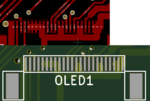
pcb-short.png

Is it OK that pins are shorted in this way or am i supposed to route the individual traces away from fpc and then short them somewhere else?
Will it affect soldering/reflow process?
 

Hi,

If your design is for a non flexible PCB, then I see no problem.

Klaus
 

Is solder mask needed in such case? i am worried what will happen if there is none. by default the kicad has minimal soldermask web width set to 0.25mm, i had to lower it to 0.1mm, which is absolute minimum what fab house can do. but i've seen reccomendation to don't use solder mask at all in such cases...
 

Hi,

usually the connector manufacturers provide design guides.

Klaus
 

Just for the record: Board came out great, the soldermask separates the pads enough. But there are three minor issues with this approach.

TLDR: if you want perfect board, don't do this. otherwise you are probably OK.

1.) The pads shorted by wide trace like this have higher thermal capacity, so i've experienced cold joints without continuity on two of the shorted pads when i was soldering it using manual hot air method. So i had to reheat it with fine tip iron and add bit of solder to fix these. No big deal, but it wasn't immediately obvious during visual inspection under microscope (to my untrained eye).

2.) Shorted pads are bit wider due to solder mask relief/clearance, which makes them tend to create solder bridges across those pins (but they are already supposed to be shorted anyway, so it's just visual problem)

3.) If you don't remember which pins should be shorted, you can't really tell with connector and solder bridge in place, so you might end up spending time removing solder bridges from pins that are shorted anyway. if you route the short away from connector, you can easily tell that it's ok to have bridge over these pins.
 

Status
Not open for further replies.

Part and Inventory Search

Welcome to EDABoard.com

Sponsor

Back
Top