Continue to Site

Welcome to EDAboard.com

Welcome to our site! EDAboard.com is an international Electronics Discussion Forum focused on EDA software, circuits, schematics, books, theory, papers, asic, pld, 8051, DSP, Network, RF, Analog Design, PCB, Service Manuals... and a whole lot more! To participate you need to register. Registration is free. Click here to register now.

folded cascode biasing

Status
Not open for further replies.

deep_sea

Advanced Member level 4
Full Member level 1
Joined
Oct 23, 2019
Messages
100
Helped
14
Reputation
28
Reaction score
18
Trophy points
18
Visit site
Activity points
855
Hello fellows,
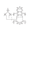
I am wondering how to generate the biasing voltages of folded cascode (VG3,VG5,VG7,VG9)?
How to determine which voltage levels should be there and what circuit to generate?
I have tried current mirror for PMOS part but how to bias NMOS part?
Thanks in advance,
 

Attachments

  • CMOS-fully-differential-folded-cascode-opamp-with-a-large-step-applied-at-the-input.png
    CMOS-fully-differential-folded-cascode-opamp-with-a-large-step-applied-at-the-input.png
    11.8 KB · Views: 1,098

Thanks for your reply. I know that transistors are biased by current. What I ask is do I need two current mirrors? Let us talk in more details.
Assume pmos input pair biased by a tail wide swing cascode.
Now the drain of this pair is connected to a drain of an nmos (M4). M4 should be biased by (2*IB) for example. Should I use another wide swing current mirror to bias it? In this case, the cascode voltage should be the voltage of the wide swing cascode.
What about the load part? Should I use a third current mirror to bias the PMOS cascode load?
 

Thanks sutapanaki for ypur reply.
I have attached a possible biasing scheme for single ended output folded cascode.
The wide swing cascode current mirror is used to bias the tail current source with 2*Ib. The same current mirror is used to bias the mirror load with Ib through VB3 and VB4.
For the NMOS side, M2a,b were guaranteed to be in saturation by connecting its gate to the drain of M3a,b. For M3a,b to be in saturation, a resistor is used to have a certain VGD below Vth. A similar resistor is added to the output side for balance. It might be not necessary if balance is not required.
There are common mode feedback circuits that could be used also for biasing, in particular in fully differential OTA.
 

Attachments

  • folded_cascode_w_bias.png
    folded_cascode_w_bias.png
    41.8 KB · Views: 1,629

You don't need common-mode feedback in the case of a single ended amplifier. Connecting the gates of M2a,b to the drains of M3a,b does not guarantee the saturation operation of those transistors. What guarantees it is the gate voltage and the Vov of M3a,3b.
Where did you copy this description from?
 
Last edited:

I did not copy it. I created it.
I have said exactly what you say. The Vov over the resistor from M3 drain to gate is set by the resistor value lower than the threshold voltage to guarantee saturation operation.
 

I'm sorry, I probably misunderstood what you've written. It looked to me that when you mentioned the resistor you were describing the operation of M3a.b. An what I was saying was that M2a,b were not guaranteed to be in saturation by M3a,b, being in saturation.
 
Status
Not open for further replies.

Part and Inventory Search

Welcome to EDABoard.com

Sponsor

Back
Top