Continue to Site

Welcome to EDAboard.com

Welcome to our site! EDAboard.com is an international Electronics Discussion Forum focused on EDA software, circuits, schematics, books, theory, papers, asic, pld, 8051, DSP, Network, RF, Analog Design, PCB, Service Manuals... and a whole lot more! To participate you need to register. Registration is free. Click here to register now.

Flyback Transformer Driver

Status
Not open for further replies.

boylesg

Advanced Member level 4
Joined
Jul 15, 2012
Messages
1,023
Helped
5
Reputation
10
Reaction score
6
Trophy points
1,318
Location
Epping, Victoria, Australia
Activity points
11,697
Have settle on this modification of the design:


I tried the TC4422 connected to the 12/24V rail with a 12V zenner diode in parallel with it to protect it but it appears that 24V results in the power rating of the zenner diode being exceeded followed by over voltage on the TC4422. So it would appear that zener diodes are not all that a robust way to protect the TC4422 if you want to increase the input voltage to the fly back transformer.

On the other hand a voltage regulator appears to be a far more robust way of protecting voltage sensitive components, up to a point, as it is a simple matter of attaching an appropriate size heat sink to it.

So I attached a larger than usual heat sink to my 12V voltage regulator and then a much larger heat sink to the top of this, face to face. So I should have a fairly large heat dissipation capacity for it as long as the heat transfers adequately across the junction between the two heat sinks. There is a pad of some sort between them that was mounted under the transistor that was originally attached to the large heat sink on an old tv circuit board - I guess it is an alternative to the thermal paste normally used between the electronic components and heat sinks.

Probably all very obvious to you experts though......but I am just learning.
 

The zener diode array on that schematic is a very lossy way to achive snubbing of the turn-off transient. I suggest tying a sunbber from the MOSFET drain to the power rail...diode (anode at the mosfet) to an R&C in parallel.
 

The zener diode array on that schematic is a very lossy way to achive snubbing of the turn-off transient. I suggest tying a sunbber from the MOSFET drain to the power rail...diode (anode at the mosfet) to an R&C in parallel.

It may be lossy but it is also insufficient when using a tv flyback transformer at 19kHz. I found that those zeners started smoking. I have since implemented an RCD clamping snubber. It seemed to work but the resistor got quite hot and I might have to use a higher power rating or wlaw dunk it in water.

Would you mind suggesting resistor and capacitor values of an RCD snubber that you would use................just to make sure my calculations were at least in the ball park?
 

...I tried the TC4422 connected to the 12/24V rail with a 12V zenner diode in parallel with it to protect it but it appears that 24V results in the power rating of the zenner diode being exceeded followed by over voltage on the TC4422. So it would appear that zener diodes are not all that a robust way to protect the TC4422 if you want to increase the input voltage to the fly back transformer.

On the other hand a voltage regulator appears to be a far more robust way of protecting voltage sensitive components, up to a point, as it is a simple matter of attaching an appropriate size heat sink to it.

So I attached a larger than usual heat sink to my 12V voltage regulator and then a much larger heat sink to the top of this, face to face. So I should have a fairly large heat dissipation capacity for it as long as the heat transfers adequately across the junction between the two heat sinks. There is a pad of some sort between them that was mounted under the transistor that was originally attached to the large heat sink on an old tv circuit board - I guess it is an alternative to the thermal paste normally used between the electronic components and heat sinks.

Probably all very obvious to you experts though......but I am just learning.

Several points occur to me about your design --- but the first & foremost is your use of a Zener as a "protection device".
Let's be clear about this ... a zener is not designed to be a protection device, but rather a simple way to achieve voltage stability. Connecting a 24v supply directly to a 12v zener is almost the equivalent of shorting the supply outputs. You HAVE to use a resistor in series (chosen appropriately) for the zener to do any regulation whatsoever.

Now in your published circuit, you have D2 connected at the output of the 7812xx. It serves no purpose here since the 7812 will never put out a voltage greater than the 1N4745A's 16v limit. You can delete this component entirely.

Next - you regulator should AlSO have a series resistor on its input (an not just a diode). The value of this resistor should be small enough such that when the expected current is being drawn by your 555 & TC4422 - which i suspect will be in the ~10's of mA range, then the voltage drop across the resistor is less than (24v - 12v - 7812 dropout voltage). I.e. you want to design the input voltage at your 7812 to be as low as possible (for cool running), but not so low that it is below the level where the 7812 can do its regulation job.

So lets assume you expect a max load of 100mA. Your input voltage to 7812 should typically be > 12+2. Lets chose 15v. Hence your resistor needs to drop (24v -15v) at a current of 100ma. So chose a resistor of 9/.1 = 90 ohm. The wattage of this resistor should be 2x 9 x 0.1 ~ 2watts. (The 2x is for a safety margin). You can delete the diode - or keep it there if you want some sort of polarity reversal protection.

With the resistor in place, your 7812 will now dissipate ( 15v - 12v) x 0.1 ~ 0.3watts. No need for a heatsink on it anymore !!

Lastly regd your D4..D7. Why do you need these ? Are they for MOSFET protection ? Once again, 4x 16v = 64v, whereas the MOSFET (i can barely read it as an iRF531) has a max Vdss of 60v. The zeners won't be doing much here either. You can remove these too.

Lastly - what sort of transformer are you using. You should know what that primary inductance is, so that you do not exceed the max drain current of the MOSFET. If your 555 frequency is too low, then the main current limiting element is a 1ohm resistor. With a good battery, this implies an Imax of almost 24amps ! Your resistor will surely burn up long before that.

SO, to keep the current in check, you need to have a high enough frequency on the 555.
This is how you can calculate for current --

Lets assume your primary inductance is L. (Measure it/ get it from the spec sheets)
then the current through this will follow the basic equation I = V . t / L
Where V ~24v, and t is the ON-time of your mosfet.

I won't go beyond this, because its not clear how you intend to use your circuit.
1. Are you trying to generate high voltage on the flyback's output ?
2. Why do you think you need a snubber (as mentioned in the other posts here) ?


Thanks rohitkhanna but there have been some changes to my circuit as follows:


I have added a voltage pre-regulator to cut down 36V (3 x series car batteries) to 16V which then feeds into the LM317 voltage regulator. I probably don't need it for 36V but it would allow me add another series car battery to bring the voltage supply up to 48V for the flyback transformer. I will need to be careful how far I go adding car batteries as at some point my 5W / 16V zener in the voltage pre-regulator will fry.

Any way it means my LM317 only has to deal with 16V which it cuts down to between 14V and 15V which is close to the maximum supply voltage for a 555 timer. I was using a fixed 12V voltage regulator but decided to up the voltage a little so that my TC4422 is supplying a slightly higher than 12V to the mosfet gate.

I have also followed the LM317 datasheet and implemented it as high current voltage regulator because those TC4422 are supposed to be able to supply up to 9A. I am also intending to use one voltage regulator circuit to supply 2 flyback driver circuits corresponding to 2 audio channels.

I am actually using HR power transistors from tv sets in place of the TIP50s in the spec above - I recalculated the resistors accordingly and they seem to work just fine.

Originally I set my 555 duty cycle up for 90% but I have since attached, but not soldered, R13 to R1 in order to reduce the duty cycle to about 70% to allow for better audio modulation of the 555 via its pin 5. I can remove this resistor easily if I wish and restore the 90% duty cycle.

I am also using dip 8 sockets as a means of easily swapping capacitors on the fly. There is one for the 555 timing capacitor and the other is to allow me to send pin 5 to GND via a 100nF cap or to the audio channel input socket.

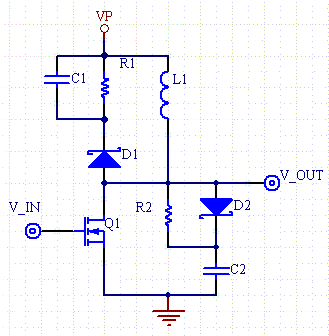
I have also gotten rid of the zener diode snubber as used in ignition coil driver kit and replaced it with an RCD snubber across the flyback transformer. The kick back voltage for a flyback transformer running at 100kHz and 36V proved to be far in excess of the kick back voltage generated by an ignition coil running at 75Hz and 12V. It is obvious to me now but it wasn't all that obvious to me at the time - I have learnt a fair bit more since then.

I have a 4 x 400V greencaps in series which add up to 85nF / 1600V and about 9 x 5W wire wound resistors in series which add up to about 1.1k. This was to spread the kick back voltage across many 5W resistors and ensure they don't burn out. I could get 1 x 100W resistor or what ever, but they are rather expensive. The snubber seems to work but any comments on it would be welcome.
 

OK, here's a comment:

Shouldn't D4 go to the drain of Q1 ?
It should also be a much faster diode than a 1N4007.

Brian.
 

OK, here's a comment:

Shouldn't D4 go to the drain of Q1 ?
It should also be a much faster diode than a 1N4007.

Brian.

I followed this website as to how to implement the RCD clamping snubber: https://www.daycounter.com/Calculators/Snubbers/Snubber-Design-Calculator.phtml
DualSnubberCircuit.gif


I only used 1N4007 in the schematic for convenience because the actual diode I used is not available. I used an ultra rectifier diode that I extracted from an old tv circuit board. It is supposed to have a reverse recovery time of 20ns or something like that. I suppose I could use a schottky diode as it only has to withstand 36V in reverse bias, while the kick back voltage of several hundred V will forward bias a schottky diode.
 

I suppose I could use a schottky diode as it only has to withstand 36V in reverse bias, while the kick back voltage of several hundred V will forward bias a schottky diode.

I suppose, the assumption is wrong. C2 will be charged up to the flyback voltage and the diode should be able to block it.
 

I suppose, the assumption is wrong. C2 will be charged up to the flyback voltage and the diode should be able to block it.

My understanding of this website is that you use one or the other type of snubber, not both at the same time.

The circuit schematic merely shows how both types of snubbers are implemented relative to the mosfet and inductor.
 

Thanks rohitkhanna but there have been some changes to my circuit as follows:


I have added a voltage pre-regulator to cut down 36V (3 x series car batteries) to 16V which then feeds into the LM317 voltage regulator. I probably don't need it for 36V but it would allow me add another series car battery to bring the voltage supply up to 48V for the flyback transformer. I will need to be careful how far I go adding car batteries as at some point my 5W / 16V zener in the voltage pre-regulator will fry.
.....

I still haven't figured out the ultimate objective of this project.
Is it to generate a very high voltage from the flyback secondary.... or is it not ?

If so, then there is really no need to have a huge (24v... 36v.. 48v) input voltage which is causing your design to get more & more complicated. The kickback voltage (if that IS what you are trying to transformer-multiply) does not depend solely on the voltage. It depends ALSO on the ratio of your PWM T-On/ T-Off times.

In fact, since T-Off is in the denominator, then focusing on better switch-off speeds will result in higher kick-back at even lower voltages.

Next - your TC4422 may be CAPABLE of 9A pulsed, but that doesn't mean it will actually NEED this current in your present design. In fact, with your chosen MOSFET (is it IRF531? IRF631? still can't tell...) input capacitance is < 800pF and Vgs(on) is 2-4v. You can switch this On/ Off in less than 25nS with just a 100mA drive !! I don't get it... why the overkilll overdesign ?

Lastly - I see you've added "audio modulation".
So is this some sort of class-D amplifier finally ?

confused... and signing out.
 

My understanding of this website is that you use one or the other type of snubber, not both at the same time.

I was referring to diode rating, not the connection differences. My comment applies to both circuits.
 

I still haven't figured out the ultimate objective of this project.
Is it to generate a very high voltage from the flyback secondary.... or is it not ?

If so, then there is really no need to have a huge (24v... 36v.. 48v) input voltage which is causing your design to get more & more complicated. The kickback voltage (if that IS what you are trying to transformer-multiply) does not depend solely on the voltage. It depends ALSO on the ratio of your PWM T-On/ T-Off times.

In fact, since T-Off is in the denominator, then focusing on better switch-off speeds will result in higher kick-back at even lower voltages.

Next - your TC4422 may be CAPABLE of 9A pulsed, but that doesn't mean it will actually NEED this current in your present design. In fact, with your chosen MOSFET (is it IRF531? IRF631? still can't tell...) input capacitance is < 800pF and Vgs(on) is 2-4v. You can switch this On/ Off in less than 25nS with just a 100mA drive !! I don't get it... why the overkilll overdesign ?

Lastly - I see you've added "audio modulation".
So is this some sort of class-D amplifier finally ?

confused... and signing out.

I am using 2SK3681 600V/43A. I also have some 2SK2611 900V/9A that I removed from some old TVs.

Put it this way...... I was using a fixed 12V regulator which all have a max current of not much more than 1A and at one stage I had one burn out on me while using the TC4422s. So it might not be drawing a full 9A into the mosfet gate but apparently it can draw enough to exceed the current rating of a standard voltage regulator. So I figured if I am going to do a high current voltage regulator, I may as well go the full hog. The power tansistors that I used were FREE anyway from old TVs. And to reiterate, I am intending to have one of these circuits driving 2 x 555 multivibrators + 2 x TC4422s.

As to 36V as opposed to 12V........I have seen many examples of high voltage arcs where people are powering TV flyback transformers and ignition coils etc with around 100V via various mains transformers. So I am assuming there must be some advantage to driving them with as high voltage as practical. But I am aware that the frequency is just as important.....which I why I am currently driving mine at 105kHz.

My intention is to create twin audio modulated HV arcs which will result in a stereo plama speaker. I will plug an ipod into them.

Eventually I will create twin tesla coils and have the driver circuits drive these instead of the flyback transformers. As far as I can tell so far this is how solid state tesla coils work, as opposed to traditional tesla coils with the spark gap and tank cap.
 

Status
Not open for further replies.

Part and Inventory Search

Welcome to EDABoard.com

Sponsor

Back
Top