xaccto
Full Member level 5

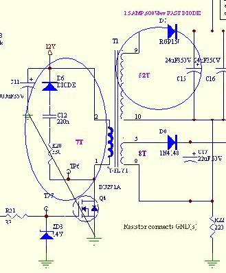
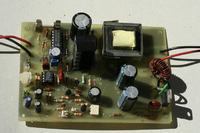
I have a simple flyback circuit as
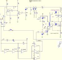
why CD4069? because I had 25 of them.
input is 10-12V, output 250V.
not exactly isolated, as I connect the grounds for 12V and 250V thru a resistor.
The feedback is using a voltage divider thru a zener diode, when the zener conducts,
a schmitt trigger switches and switches OFF the CD4069 oscillator.
The core is a bit of an unknown, looks like a ETD29, recycled off a PC board of unknown origin.
I started with an airgap by placing spacers at the legs of the core
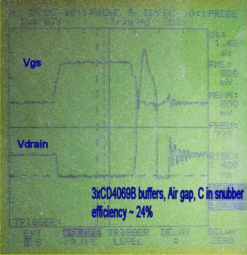
measuring efficiency by multimeter measuring current thru a load resistor, and another the volts. Power supply has volt/amp meter - questionable accuracy but lets be generous as at least 10%.
checkout the huge spike in the primary when the switch turns off
25% efficient so far.
mosfet running hottish, so is snubber diode
Ok, so no air gap......
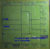
efficiency ~32%
so just checking the capability of 3xCD4069 buffers......substitute a TC427
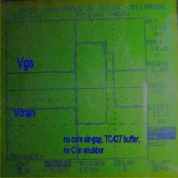
maybe slight improvement to ~35%, certainly no big improvement
C back in the snubber...
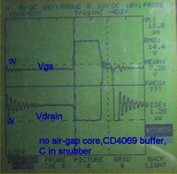
mosfet not so hot, neither is the snubber diode, but still very warmish.
the cicuit is still very protyepish, as in stray inductances etc...
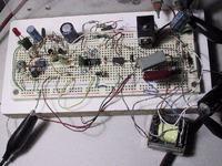
i'm disappointed, I thought should be easy to get a switcher to at least 60% efficient, but i'm stuck at half that.......
i need some ideas please
thanks

why CD4069? because I had 25 of them.
input is 10-12V, output 250V.
not exactly isolated, as I connect the grounds for 12V and 250V thru a resistor.
The feedback is using a voltage divider thru a zener diode, when the zener conducts,
a schmitt trigger switches and switches OFF the CD4069 oscillator.
The core is a bit of an unknown, looks like a ETD29, recycled off a PC board of unknown origin.
I started with an airgap by placing spacers at the legs of the core

measuring efficiency by multimeter measuring current thru a load resistor, and another the volts. Power supply has volt/amp meter - questionable accuracy but lets be generous as at least 10%.
checkout the huge spike in the primary when the switch turns off
25% efficient so far.
mosfet running hottish, so is snubber diode
Ok, so no air gap......

efficiency ~32%
so just checking the capability of 3xCD4069 buffers......substitute a TC427

maybe slight improvement to ~35%, certainly no big improvement
C back in the snubber...

mosfet not so hot, neither is the snubber diode, but still very warmish.
the cicuit is still very protyepish, as in stray inductances etc...

i'm disappointed, I thought should be easy to get a switcher to at least 60% efficient, but i'm stuck at half that.......
i need some ideas please
thanks
Last edited by a moderator:

