Continue to Site

Welcome to EDAboard.com

Welcome to our site! EDAboard.com is an international Electronics Discussion Forum focused on EDA software, circuits, schematics, books, theory, papers, asic, pld, 8051, DSP, Network, RF, Analog Design, PCB, Service Manuals... and a whole lot more! To participate you need to register. Registration is free. Click here to register now.

Floating inverter amplifier simualtion

Status
Not open for further replies.

JeremyCen

Newbie
Newbie level 2
Joined
Aug 12, 2023
Messages
2
Helped
0
Reputation
0
Reaction score
0
Trophy points
1
Activity points
43
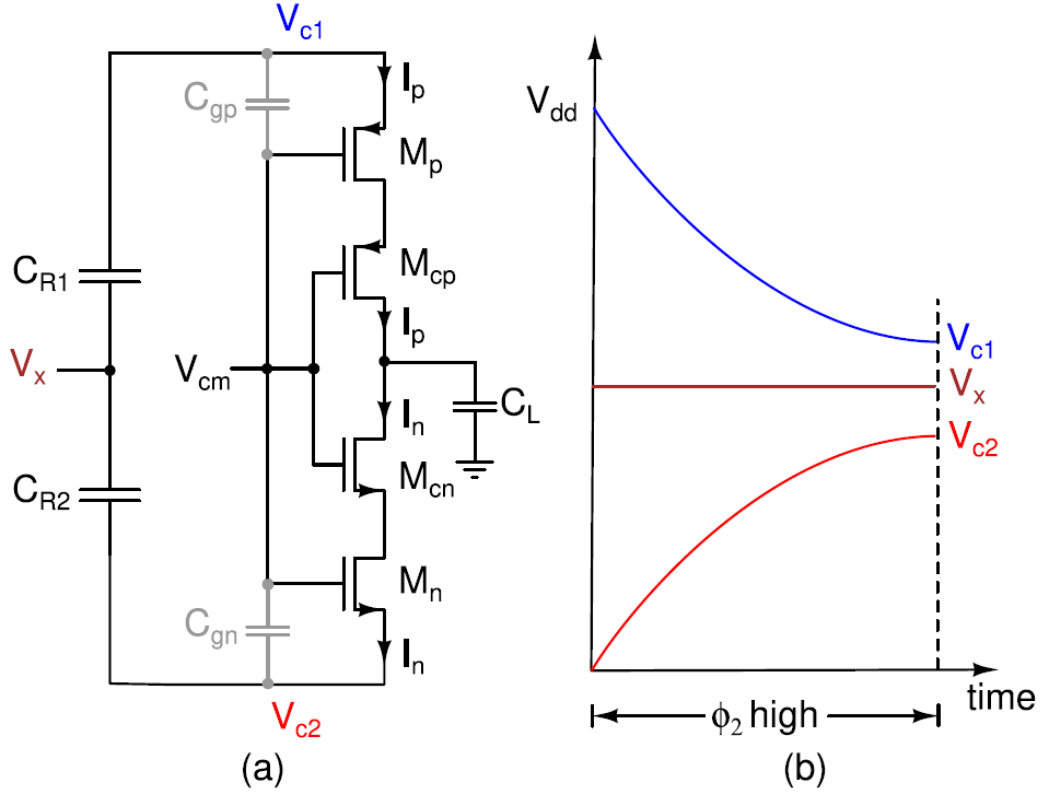
Hi all! Recently I am studying the dynamic amplifier, floating inverter amplifier (FIA). It confuses me that how can we simulate the open loop gain and phase margin that given from papers. As for FIA circuit, its operating points and supply voltage various with time during the amplification phase, which is different from the static opamp. So, I wonder do you have any experience of doing the simulation about this kind of circuit?
Many thanks!
微信截图_20230812094734.png
微信截图_20230812094810.png
 

Create two duplicate circuits, one to operate with ø1 active, the other to operate with ø2 active. If you can do so in one window then all the better.
Each simulation depicts a stage of operation.

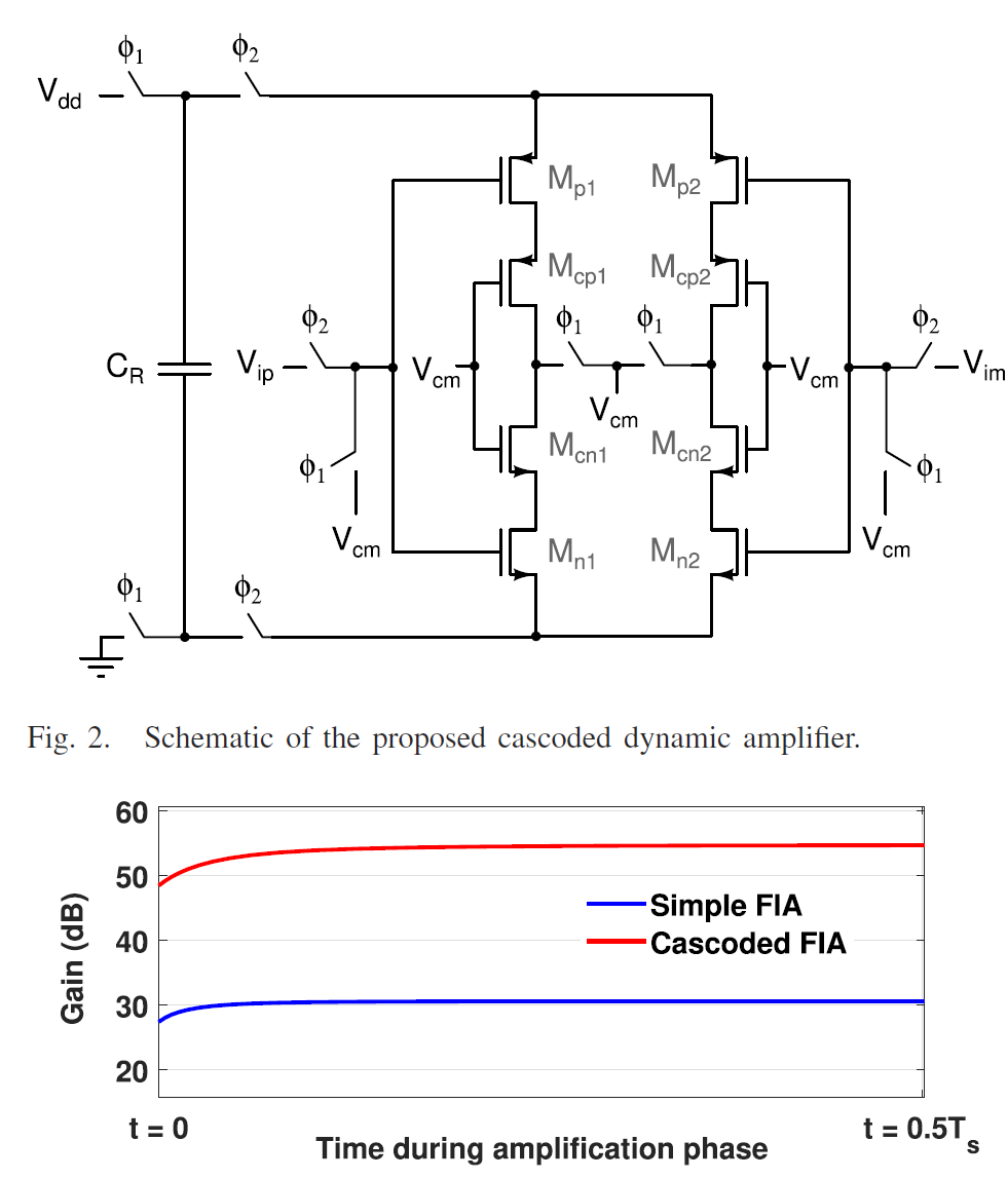
However you must determine whether there's a mistake about the first image. As printed, Ø1 closes switches so the capacitor charges from Vdd while the rest of the circuit is disconnected.

Then Ø2 occurs, connecting the capacitor so it powers the rest of the circuit. I don't understand whether: (a) this is a workaround so the layout contains at least one ground icon (because some simulators require it), or (b) whether it was intended instead to depict a reversal of supply polarity, rather than a non-changing supply polarity?
Hi, thanks for your reply.

Images are correct I think. As Ø1 close, the reservoir capacitor CR is charged from VDD, while the input & output of the amplifier are both reset to VCM. In this moment, sources of input cmos transistors are disconnected to supply.

While during the amplification phase Ø2, I think that supply polarity doesn't change. The capacitor CR powers the inverters based amplifier. Since CR acts as a floating battery, the current leaving the top plate of CR must equal the current that enters the bottom plate, which can make the output common-mode voltage stable.

However, during Ø2 period, the supply voltage of Vc1 & Vc2 is changing. I'm confused that when we design a FIA, how can we simulate FIA's dc gain & phase margin? Or should I just assume that FIA's supply is fix, for example connected to VDD? Then we can do the ac and dc simulation in cadence like designing a conventional amplifier? (since the first image indicates that the dc gain stay almost constatnt during the Ø2, we may use the initial condition for design?

Thanks again.
 

This simulation looks like your first image although I don't know if I understand everything correctly. I drew it in Falstad's animated interactive simulator. By hooking up a battery, positive current is identical to negative current.

falstad.com/circuit

As I suspected, the circuit acts in a sensible manner during Ø2. That is when input signals are amplified. Common mode is rejected.

During Ø1 the switches apply Vcm (common mode?). Current goes to maximum in left & right totem stacks. It lets us compare one mode to the other.

floating inverter amplifier at Edaboard Aug 2023.png

--- Updated ---

By clicking this link:


1) Opens website falstad.com/circuit
2) Loads my circuit into the simulator
3) Runs it on your computer.

Select Toggle Full Screen (under File menu).
Click and drag upwards on Scope area to expand its size.
 
Last edited:

Status
Not open for further replies.

Part and Inventory Search

Welcome to EDABoard.com

Sponsor

Back
Top