Continue to Site

Welcome to EDAboard.com

Welcome to our site! EDAboard.com is an international Electronics Discussion Forum focused on EDA software, circuits, schematics, books, theory, papers, asic, pld, 8051, DSP, Network, RF, Analog Design, PCB, Service Manuals... and a whole lot more! To participate you need to register. Registration is free. Click here to register now.

First PCB build help.

Status
Not open for further replies.

WBrumble

Junior Member level 3
Joined
Nov 13, 2015
Messages
26
Helped
0
Reputation
0
Reaction score
0
Trophy points
1
Activity points
261
All,

This is my first PCB build and I've got some questions before finalizing and moving to fabrication.

It's a 2 layer board, with led drivers (for RGBW), 12 volt supply, LED drivers running at 2mhz, and a maximum of 4 amps, 1 amp per color die.

The inputs at the bottom are; White, Red, Green, Blue are PWM inputs, and VCC/GND.

Board outline dimensions 3 3/16"x 3"

Two questions I have:

- Do I need to worry about EMI at 2mhz?

- What spacing for ground vias do I use between to top and bottom layer ground pours?

One more question not really related directly to the PCB design, could someone point me to a good read for thermodynamics and heatsink calculations/design.

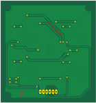
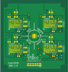
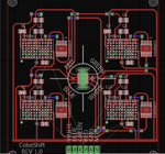
Here are exported photos from eagle of the top and bottom of the board "if you see any issues please let me know":
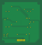
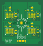
eagleUp_Light_Bar_board_bottom.pngeagleUp_Light_Bar_board_top.png

Thank you guys in advance for the help!
 
Last edited:

Yes, you need to worry about EMI. It's the rise-time of the edges that causes the problem, not just the frequency.
 

Barry,

It's just hobby level, and my first build. But, I like to challenge myself to learn and do the job right, it's more satisfying when your finished and you also learn a lot while doing it that way.

Are there any rule of thumb calculations and practices that will keep the EMI within compliance?

Thank you for your reply.
 

What compliance? FCC? EU? If it's just a hobby circuit then why are you concerned with compliance? A few rules are: slow down rise and fall times; use a ground plane; use ferrite beads where necessary. Professionals design circuits and follow the 'rules' and still don't meet compliance the first time.

You asked if you "need to worry". That depends on what you're afraid of...
 

A schematic would really help with this.

Either you have the labels on the connector wrong or you do not actually have a groundplane.
You have it so that VCC is the top area of copper pours and the bottom that is connected to GND is so small it's pointless.

Look hard at your GND tracks, the return currents must return straight to the input not meander via thin slithers of copper because poor routing forces them thin nor through vias when its easy to make it a single piece of copper.

As it's a hobby board, is there any specific reason for that pinout on the connector?
Can you re route the connections into it so that the GND flows straight upwards?

Sort out the connections and reroute them so you can achieve this.
Bottom.png

Also the thin slither that goes nowhere is rather pointless, either get rid or thicken it and try and join it at the other end.

Top.png

The GND return for the bottom RH LT8042 comes from the bottom of the board all the way to the top then down again, reroute the tracks so that it goes direct.
The left side LTM IC's do not even have a GND connection, they are connected to floating copper.

And if you look on the bottom, you have a thick track running horizontally across the middle making a big slot in your gnd that will cause the return currents to go via the thin bits.

Me, I'd reroute it to improve the gnd flow - but for a hobby board it will likely work as long as you get 100% connectivity to the GND (which I cannot see being so at present).

Also https://www.edaboard.com/forums/15/ is the PCB routing forum :)

MS Paint does not do the pics well lol
Have a merry sherry new year.
 

I'm an service electrician on drilling rigs, when spec'ing anything there are rules and regulations that make sure the job gets done right and that it's safe.

I follow the NEC and IEC here in America, I'm not sure who regulates the PCB design world, but I want to follow their standards to make sure all the projects
I'm working on get done right and safe.

The do I need to worry, was about EMI.

Since this is my first dive into the PCB design world, even at a hobby level, I want to learn the correct way of doing things so that I don't develop bad
habits that I will have to un-train myself later on down the road.

What I was thinking on the top layer was for heat spreading, I have vias connected to the bottom ground plane, then the connection is made at the PTH hole connection on the bottom, or would it be better to connect the bottom and top pours to the PTH?

Routing the traces without dropping to the bottom layer while keeping the PCB small, and current traces short is a PITA! Ha ha. But I see now the radiating current has to go around slots if you run traces through the bottom ground plane.

Some stuff I've dug up while google'ing, Image planes, the 20 x H or 100 x H rule, multi point and single point grounding, and partitioning.

The VCC plane is big and goes left and right, to handle the current and heat dissipation is what I had in mind.

I thought about putting this post in that section but after some thought I was thinking that section is related to software issues with design programs.

Thanks for the help guys! Appreciate you taking the time to help a noob out.

PS: Attached the SCH and BRD files, and a source for EMI tips you can let me know if it's good advice or not.

View attachment Desktop.zip
 

All,

Question on the grounding.

With four different ICs controlling four different dies on one LED makes it impossible to put image ground plane under where the current flows through each IC without creating ground loops.

Any advice on how I can have four separate ground pours under each IC and then taking each of those to the common ground connection on the PTH connector, and the best way to avoid radiating the current due to the separated ICs?

Thank you all again!
 

All,

Re-routed it, took out the power planes, and tried keeping everything off the bottom plane.

EMI Question2.png

Do I need to separate the four ICs on the bottom layer ground pour, will connecting all of them together with a copper pour on the bottom create ground loops?

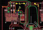
EMI Question.png

With four of these it's like impossible to route the power traces to the LED without them having to cross.

Orange is the input for the current to the IC.

Green is the return current path.

Yellow highlights the points to some questions I have with routing it like this.

1) Is the gate signal to the FET, should be okay routing under like that?
2) Is it okay for power traces to cross like this? Will be pulling 1 amp maximum.
3) Is it okay for a power traces for the other LED die to cross under like this?

In advance thanks to all who help me!
 

Henry Ott, Ralph Morrison and Keith Armstrong for EMC stuff.
A PDF schematic would be a great help...
One single ground plane, nothing else would be best and preferably contiguous.
 

Here is a very good list of EMC tips for PCB
 

Attachments

  • henry ott pcb_guide.pdf
    10.5 KB · Views: 106

Status
Not open for further replies.

Similar threads

Part and Inventory Search

Welcome to EDABoard.com

Sponsor

Back
Top