Continue to Site

Welcome to EDAboard.com

Welcome to our site! EDAboard.com is an international Electronics Discussion Forum focused on EDA software, circuits, schematics, books, theory, papers, asic, pld, 8051, DSP, Network, RF, Analog Design, PCB, Service Manuals... and a whole lot more! To participate you need to register. Registration is free. Click here to register now.

finding footprint of certain connector

yefj

Advanced Member level 5
Joined
Sep 12, 2019
Messages
1,505
Helped
1
Reputation
2
Reaction score
5
Trophy points
38
Activity points
9,114
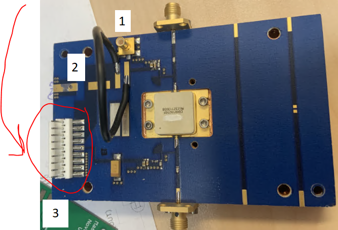
Hello, in the datasheet shown below J3 is HEADER RT>PLZ .1CEN LK 9POS what is the exact name of the connector so i could find it in digikey?
Thanks.
https://cdn.macom.com/datasheets/CGHV1A250F.pdf
1710159885251.png
 
Looks like a generic 0.100" (2.54mm) spacing, right-angle, SMT, connector.

Your data sheet is for a transistor, it has nothing to do with the connector.
 
The connector actually looks like a JST-EH-9 connector.
--- Updated ---

Take a look at 640457-9 at digikey website.
 
Last edited:
Last edited:
Hi,

What´s the units of the measurement tool used in post#3?
Instead of using a measurement tool (I´ve never seen) you could do the measurement and post the values. I mean: you need them anyways to do a useful search... and to compare with datasheets.

And please post a photo as side view of the connector. (100kB should be sufficient)

Klaus
 
Hello Klaus , in post 3 i put 10mm ruler next to the connector.
In this board they put a connector which is intended to threw hole on a surface mount foot print.
I need to download a foot print where i could do the same trick as shown in the photo below.
does the footprint shown in the link below will do the job?
i need the pads size and position to fit the metal going on top of it.
What footprint you recommend for my purpose?
Thanks.

https://eu.mouser.com/ProductDetail...X3*MTcxMDIzNjcxNS4xLjAuMTcxMDIzNjcxNi4wLjAuMA..

1710237389106.png
 
I need to download a foot print where i could do the same trick as shown in the photo below.
Download? This means you are not able to put 9 SMD pads in a row on your own????

Please focus on what you do: (maybe it´s time to take a sleep)
* don´t post a link to a transistor while you talk about a connector (post#1)
* don´t talk about resistors (post#5)
* there is no "footprint in the link below" it shows a selling site for a different connector

PNG is not useful for photos --> use JPG

(PNG is useful for screenshots with limited count of colors, like diagrams, schematics, ...)

Klaus
 
Hello Klaus, you are correct :) It easier to build it by myself.as shown below.
1710247219683.png
 
Last edited:

LaTeX Commands Quick-Menu:

Part and Inventory Search

Welcome to EDABoard.com

Sponsor

Back
Top