Continue to Site

Welcome to EDAboard.com

Welcome to our site! EDAboard.com is an international Electronics Discussion Forum focused on EDA software, circuits, schematics, books, theory, papers, asic, pld, 8051, DSP, Network, RF, Analog Design, PCB, Service Manuals... and a whole lot more! To participate you need to register. Registration is free. Click here to register now.

Ferrite bead usage in ADC's

Status
Not open for further replies.

decaf14

Newbie level 5
Newbie level 5
Joined
Jul 15, 2019
Messages
10
Helped
0
Reputation
0
Reaction score
0
Trophy points
1
Activity points
173
Hello,

I'm a novice PCB designer doing my first mixed-signal board for a thesis project.

I'd like to digitize a signal and was planning to use the ADS1115 ADC in conjuction with the SAMD21G18 microcontroller. I've chosen the ADS1115 specifically because adafruit has a hardware reference design. I noticed in their reference design that they have an odd configuration using ferrite beads. They place a ferrite bead between two grounds to "isolate" one from the other. From what I can infer online, isolating power supplies with ferrite beads is good, but isolating grounds is bad.

Can anyone advise me on this? Please see the attached schematic of the ADS1115 breakout board from adafruit. Note the ferrite bead connections between system ground and system power.

adafruit_layout.PNG

This is my Altium schematic where I've mimicked adafruits design.
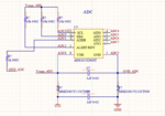
my_layout.PNG

Thanks.
 

I've never seen anything like this before with the bead in the ground path. I can't think of any reason for it. I would think it would hurt rather than help. But you can always replace it with a jumper.
 
Hi,

I agree, too.

Klaus
 
This kind of filter only would make sense if it were made with a common mode choke, but both component designators FB1,2 are clearly for distinct (uncoupled) devices. It is likely someone copied the diagram of another circuit making changes without knowing exactly how it works.
 
Thanks everyone. I'll leave the 0402 ferrite bead option open in case anything acts up but I won't solder it initially and won't solder it unless I'm seeing a lot of noise.
 

Sometimes bead placement is "what worked" and nobody
knows exactly why.

Signal ground and power current return don't necessarily
want to be the same thing. Who's contaminating who?
If the main ground plane is filthy, maybe standing off the
HF but keeping the DC potential right, is the magic tweak.

Whatever "noise" is on the power supply, is also on "the"
ground. You just don't see it so well when that's also your
'scope reference. But every decoupling cap's job is to scrape
off the HF current from the supply and shunt it to ground -
so there's likely plenty of circulating HF trash, and maybe
you'd be better off not seeing it. Clean source and filthy
reference ground is no better than filthy source and clean
ground.

It might not be a waste of time to track down the designer
of this "reference design" and ask them why the ferrite bead,
and what to look for as consequences of removal. It could
be some obscure thing that you'd miss (but your customers,
perverse bastages that they are, will find on Day 1).
 

To me, the ground ferrite bead in the Adafruit board breakout board doesn't make much sense. I don't believe that the board has been designed by an analog or mixed signal expert.

If you look for reference designs, consult Texas Instruments web site.

The board doesn't have a separate analog ground, thus any voltage drop along the ground ferrite is superimposed to the analog input signal. Operating the I2C interface injects noise to the analog input etc. The ADC must be operated exclusively in differential mode to get rid of this interferences.
 

The ferrite bead prevents RF from the digital circuitry from getting coupled to the analog side.
OP's SAMD21G18 will generate up to 48MHz hash+harmonics on DGND which you do not want on your AGND.
A ferrite bead joining two grounds (analog and digital) is common practice and discussed in Analog Devices app notes. Usually used above 20-bit resolution for ADC and DAC use.
If you don't believe in it, then just put a 0R in place. This will put you in the "ground everything together" camp which is another approach to grounding mixed-signal circuitry.

The need for it shows up with long field wiring to analog sensors and such, conducted emissions are terrible as the cables are essentially antennas radiating the MCU's emissions from DGND.

Also note the ferrite bead approach fails if your decoupling caps are connected the wrong ground, i.e. when the ADC is powered from DVDD so the cap can essentially bypass the ferrite bead and defeat its purpose.
The Adafruit board is not a good design.
I don’t know what schematic YOU’RE looking at, but there’s only one ground on this one, that’s why the OP’s original question. There’s no separate grounds. There’s no caps “connected to the wrong ground”. There’s no “long field wiring”. You’ve answered some totally different question.
 
  • Like
Reactions: FvM

    FvM

    Points: 2
    Helpful Answer Positive Rating
I read this in OP's post and thought I'd answer that question:
"... They place a ferrite bead between two grounds to "isolate" one from the other... Can anyone advise me on this?... "
It's on Adafruit's ADS1115 schematic other ADC app notes.
 

The ferrite is to provide some attenuation to any noise coming in of the connector JP1, often used with a moat, that the ferrite bead bridges. More often a common mode choke is used for all signals, but I have seen this and used this technique, mainly on some mill stuff.
 

I addressed the problem of the Adafruit board in post #7. It doesn't implement separate analog and digital grounds, just a series ferrite bead in the single ground line. Respectively noise is superimposed to the analog inputs.

We don't know how this problem would be handled in the post #1 circuit, it doesn't show the analog input signal ground reference. Because Adafruit is quoted as reference, we can just guess that the OP isn't aware of the involved problems.

Regarding "common practice" of separated grounds and Analog Devices application notes. These recommendations look good on evaluation boards that have one and only one mixed signal chip where you can place the connecting ferrite bead or jumper directly between analog and digital pins of this chip.

Real world mixed signal designs have multiple ADC and DAC. How to place the ferrite bead(s) in this case? Without creating unwanted ground loops and exceeding the maximal AGND to DGND voltage difference?

From time to time I'm engaged with fixing EMI related faults in other peoples designs. I remember bad designed ground separation as a popular cause of unwanted RF susceptibility.
 

It is filtering the supply going into the Adafruit board, the OP's schematic is wrong and he has interpreted the circuit diagram of theAdafruit board wrong, it is nothing to do with the on-board GND...
!!!
 

It is filtering the supply going into the Adafruit board, the OP's schematic is wrong and he has interpreted the circuit diagram of theAdafruit board wrong, it is nothing to do with the on-board GND...
!!!

Nope. The OP is not wrong, he is showing the exact schematic for the Adafruit board. It has EVERTYHING to do with the on-board ground.
 

I grumble about Adafruit's intentions because putting a ferrite bead between system GND and the ADC GND doesn't work here- because the ADC IC only has one ground pin. The result is digital currents (SPI) have a high Z return path to the system (DGND), which you do not want. It's very easy to check with a scope or spectrum analyzer if that ferrite bead makes things better or worse.
Pic shows how it is properly done on a 24-bit DAC IC, which has separate DGND and AGND pins with a ferrite bead L5 joining the two.
AD1955 DAC ground.PNG


Follow up - I measure 16 ohms between AGND and DGND on the AD1955 DAC IC. In the ADI Engineer Zone forum, the EVAL board designer says the two grounds are connected to a ring on the die. So I am wrong about splitting the two grounds with that part- although AD did that in earlier EVAL board revisions which is confusing. I cannot find the schematics/docs for the latest AD1955 EVAL board in the public domain.
With another DAC IC CS4398 I get no continuity, only a substrate diode between AGND and DGND.
So with these IC's grounding is done differently it seems.
 

Hi,

You don't want high currents between GNDs on a die. Thus the chip designers use a relatively high ohmic path ... just to avoid high voltage difference.

The PCB designer needs to design a suitable GND concept.
Both GNDs need to be connected with low impedance ... at a suitable location.

But a ferrite bead is an inductance..it is no low impedance at high frequencies.
(Thus I'd prefer a wire)

Instead of using a ferrite bead ... I assume a solid GND plane is more effective.
For sure a split (in the) GND plane can improve this .... as long as you know where to place the split.

And two separate GND planes may be an improvement over a single GND plane .... as long as you know where you connect them.
But be aware that two GND planes next to each other will be capacitively coupled.
I cannot find the schematics/docs for the latest AD1955 EVAL board in the public domain
Both schematic as well as PCB layout is given in the eval board user guide.

Klaus
 

I cannot find the schematics/docs for the latest AD1955 EVAL board in the public domain.
Any indications that a newer version than Rev.0 linked in my previous post exists at all?

With another DAC IC CS4398 I get no continuity, only a substrate diode between AGND and DGND.
So with these IC's grounding is done differently it seems.

Nevertheless, the datasheet has a clear suggestion:
The AGND and DGND pins should be tied together with solid ground plane fill underneath the converter extending out
to the GND side of the decoupling caps for VA, VD, VREF, and FILT+.
 

EVAL-AD1955 webpage offers no schematic or user guide that I can find. Nor does Digikey or Mouser, who sell the EVAL board for $555. They must have changed the grounding strategy at some point, but I have no way of knowing aside from that URL you gave. How did you find it?
The Analog Devices document I have EVAL-AD1955EB Rev. 0 2002/05 has a pcb layout with split-ground and 600Z ferrite bead between them.

Now I'm confused, as there are ADC/DAC designs with a split ground (AGND, DGND) and either a single point (star) ground with copper or a ferrite bead joining the two. I've done it to lower conducted EMI from DGND into AGND. If you have a fast MCU, I have seen GHz harmonics on DGND which you do not want radiating out to field wiring to sensors etc. on the analog side, having a dirty AGND.
But it seems to depend on the ADC/DAC IC's (die) design, if there are one or two grounds.
 

Status
Not open for further replies.

Part and Inventory Search

Welcome to EDABoard.com

Sponsor

Back
Top