Welcome to our site! EDAboard.com is an international Electronics Discussion Forum focused on EDA software, circuits, schematics, books, theory, papers, asic, pld, 8051, DSP, Network, RF, Analog Design, PCB, Service Manuals... and a whole lot more! To participate you need to register. Registration is free. Click here to register now.
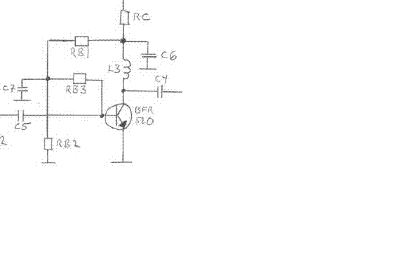
To me it looks like a bias circuit for a class A amplifier as it will make a "stiff" bias-point. You can adjust the base and collector voltage with the resistors. The idea is that it is stable against such things as temperature variations because it is self regulating the base-emitter voltage.
Bipolar transistors use more current as the temperature rise. This circuit will counter act this becuase the voltage collector will drop and this will also lower the base voltage which then lowers the collector current and so on...
The values of the inducor and capacitors depends on frequency.
Almost, but one important feature missing, tyassin.
The combination of RB3 and C7 determines the AC impedance between the base of the transistor and ground.
This arrangement would be used when the Thevenin equivalent (in this case the value of RB1 and RB2 in parallel) of the DC divider is well above that desired for the AC signal. SO A small value - RB3 - is inserted and C7 shunts the AC to ground thus defining the impedance at the base.
Thanks folks for your replies.
But I was actually expecting the explanantion of the operation of this circuit.
For example, why the resistor R3 is not connected directly next to the base and y a separate branch fr that.
If you know the operation of it, you can very well reply to this post.None is forcing you to reply for this post.
If you find this so silly and childish, u can very well go and visit other posts rather than writing your own opinion about the post in an irrelevant manner.
Dont discourage people if you dont want to answer atleast..!
Santom
[ comment by moderator. The reply referenced in this comment has been deleted due to impoliteness. Many people with some misconceptions about science and technology trust this board to supply their missing knowledge without insults. I admire people who are willing to expose their lack of knowledge in the quest to have perfect knowledge from others coaching them.]
I think a student should at least attempt to describe an unknown circuit. An attempt was not made.
Don't you think that L3 is just a short piece of wire at DC?
Then do you see than RB1 and RB2 form a voltage divider of the DC voltage at the collector of the transistor?
Then RB3 applies base bias with DC negative feedback so the transistor's operating point will not change much if a high gain or if a low gain transistor is used?
Do you see that C7 filters the signal to ground so that there is no negative feedback signal to the base in order to keep the signal's gain very high?
This site uses cookies to help personalise content, tailor your experience and to keep you logged in if you register.
By continuing to use this site, you are consenting to our use of cookies.