Tenatious
Newbie level 3

I'm looking at making my UK light switches "Smart" and controllable via Wi-Fi and have come up with the following and wanted some advice on what I have so far: namely, will it work as I think it will and secondly is it safe the way I have gone about doing it or are there any other suggestions people have to making it even safer, don't want to get a nasty shock!
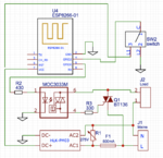
The idea is to keep my regular light switch as they are expensive stainless steel plated switches and I don't want to replace them with tacky Wi-Fi switches like the LightWave RF or Sonos T1 and then use this light switch as an input in to an ESP8266 GPIO. This way the light can be controlled both by the physical switch or via Wi-Fi and won't cause any issues should the Wi-Fi decide to die. When it senses a change in the GPIO the program will power an optocoupler which will in turn power a triac causing the light to turn on.
Standard switch is connected as in the schematic. Negating the pull up resistor required as the GPIO pin is set to 'INPUT-PULLUP' and so will just notice a change from either 3.3v to GND when the switch is used.
I want to make use of the mains 240V powering both the light and the ESP8266. I have a neutral wire in my sockets unlike most of the UK. To achieve the mains powering the ESP8266 I have opted for a HLK-PM03 240V - 3.3V supply.
Let me know your thoughts please


