Continue to Site

Welcome to EDAboard.com

Welcome to our site! EDAboard.com is an international Electronics Discussion Forum focused on EDA software, circuits, schematics, books, theory, papers, asic, pld, 8051, DSP, Network, RF, Analog Design, PCB, Service Manuals... and a whole lot more! To participate you need to register. Registration is free. Click here to register now.

Error/Warning in DC convergence in Cadence Spectre

theguardian2001

Newbie level 6
Newbie level 6
Joined
Sep 29, 2024
Messages
11
Helped
0
Reputation
0
Reaction score
0
Trophy points
1
Activity points
164
Hi everyone! I can say that I am relatively new in Cadence and I am currently migrating there from Spice. I was trying to simulate a dif. amplifier in gpdk90nm and have run into some problems. First of all, when I tried to simulate the schematic it has run into convergence errors and inability to compute an operating point (please see spectre_1.out in attachment). I am also attaching a log file (Job5) in case it is needed.

After several attempts I created a cellview from my schematic and provided power and input connections "on top" of it (by placing the created cell into a new cellview). The same simulation completed without any errors but the warnings appeared are crucial for the design:
Warning from spectre.
WARNING (CMI-2477): I0.PM0: `Rds' = 433.574 nOhm is less than 0.001. Set to 0.
WARNING (CMI-2477): I0.PM1: `Rds' = 15.9184 uOhm is less than 0.001. Set to 0.
WARNING (CMI-2477): I0.PM8: `Rds' = 867.631 nOhm is less than 0.001. Set to 0.
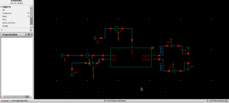
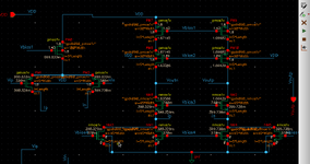
This basically implies that PMOSes does not contribute to output impedance thus ruining the overall gain. (Please see spectre_2.out). I would really appreciate any help and hints which can help me (and probably others in the future) to resolve the issue. The schematic is attached as a picture as well (Constant voltage sources were placed instead of a full bias circuitry - which has been tested without errors but with the same warnings - to reduce the complexity of the netlist file).

In case if anybody knows what causes Spectre to run the simulations with a symbol but not the schematic and why do only 3 PMOSes suffer from from low output impedance - I would also highly appreciate any explanation or advice regarding this issue to be able to resolve it in future.

Thanks everyone in advance
Folded_cascode.png
 

Attachments

  • spectre_1.txt
    1.6 MB · Views: 31
  • Job5.txt
    5 KB · Views: 37
  • spectre_2.txt
    11.5 KB · Views: 32
I suppose you have solved the issue already.

For future interaction: I guess we need to see the test bench with the symbol option too. A netlist in addition to the run logs would also make sense.
What are the variables, Width and Length, for example, in the two simulations.

I also suspect that something is set up wrong with units/voltages. The transient time, for example, indicates Ts (as in 10^12 s) run times.
 
Hi, jjx! Thanks for your reply.

Unfortunately, I a still struggling with this issue and as before would appreciate any reasonable comments under this thread. I got some feedback regarding the model files from cadence community: https://community.cadence.com/caden...-2477-rds-is-less-then-0-001-gpdk90nm/1401359

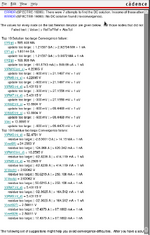
I also took a closer look at a log file and convergence errors simulator is facing. It somehow comes with voltages far above the supply and GAmpers currents through the constant dc sources which are connected to the gates

Code:
Top 10 Solution too large Convergence failure:
    I(V6:p) = 585.468 MA
        update too large:  | 1.21597 GA | > 2.92734 MA + 1 nA
    I(V1:p) = 1.80144 GA
        update too large:  | 1.21597 GA | > 9.0072 MA + 1 nA
    I(V2:p) = 169.938 mA
        update too large:  | -81.8793 mA | > 849.69 uA + 1 nA
    V(PM10:int_s) = 4.22995 V
        update too large:  | -600 mV | > 21.1497 mV + 1 uV
    V(PM8:int_s) = 4.22995 V
        update too large:  | -600 mV | > 21.1497 mV + 1 uV
    V(PM9:int_d) = 5.43115 V
        update too large:  | -300 mV | > 27.1558 mV + 1 uV
    V(PM7:int_d) = 5.43115 V
        update too large:  | -300 mV | > 27.1558 mV + 1 uV
    V(NM2:int_s) = 13.8894 V
        update too large:  | -600 mV | > 69.4468 mV + 1 uV
    V(NM0:int_s) = 13.8894 V
        update too large:  | -600 mV | > 69.4468 mV + 1 uV
    V(in) = 13.8895 V
        update too large:  | -600 mV | > 69.4476 mV + 1 uV
 Top 10 Residue too large Convergence failure:
    V(PM0:int_d) = 52.4731 V
        residue too large: | -2.83001 GA | > 14.15 MA + 1 nA
    V(net01) = 34.2983 V
        residue too large: | 124.068 A | > 620.342 mA + 1 nA
    V(PM10:int_d) = 10.2595 V
        residue too large: | -82.8239 A | > 414.119 mA + 1 nA
    V(PM8:int_d) = 10.2595 V
        residue too large: | -82.8239 A | > 414.119 mA + 1 nA
    V(Voutn) = 2.63062 V
        residue too large: | 50.6215 A | > 253.108 mA + 1 nA
    V(Voutp) = 2.63062 V
        residue too large: | 50.6215 A | > 253.108 mA + 1 nA
    V(PM7:int_d) = 5.43115 V
        residue too large: | -32.9025 A | > 164.512 mA + 1 nA
    V(PM9:int_d) = 5.43115 V
        residue too large: | -32.9025 A | > 164.512 mA + 1 nA
    V(net027) = 2.56811 V
        residue too large: | 17.4373 A | > 87.1863 mA + 1 nA
    V(net029) = 2.56811 V
        residue too large: | 17.4373 A | > 87.1863 mA + 1 nA
(I assume that MOSFET model treats any gate as a high impedance node). I rearranged the symbols in the schematic so now it is probably little bit clearer which symbols have been used (Width and lengths for transistors are scaled up to 100nm as could be seen from the attached testbench). I am also attaching testbech with a netlist together with a log file part which prevents the conversion.

Again, as something which is not clear to me why do this errors do not appear for the cellview test (which can also be found in the attachments) where all the parameters and nodes stay the same without any modification.

I would assume that there is some simulation option which I probably have to set or reset to force the circuit into some "adequate" operation mode.
 

Attachments

  • Cellview.png
    Cellview.png
    28 KB · Views: 33
  • Convergence.png
    Convergence.png
    82.5 KB · Views: 40
  • schematic.png
    schematic.png
    30.5 KB · Views: 39
  • testbench.png
    testbench.png
    57.4 KB · Views: 34
GA or MA or kA are incredibly high and need to be brought down to realistic values. Either by installing safety resistors or by reducing amplitude of voltage sources. Afterward neighboring circuitry should behave.

Certain simulators might respond differently to these situations with different alerts or none at all.
 
Intriguing... can you post the input.scs netlist too, please?
(display netlist and grab the text from there...)
 
It seems peculiar to see 15V intermediate solution node voltages off a 1.8V supply.

It's also peculiar to see "pmos1v" which I'd take to mean 1V rated and possibly not well modeled outside that

Setups that create hysteretic behavior (like swapping + for - inputs) are intrinsically not single-solution within the dead band.

The same might be true of an op amp that leaves its proper input or output common mode range.

Exercising the amplifier DC open loop might reveal stuff.
Hi, dick_freebird and thanks for your comment! I have been able to set and test circuits for gpdk90 with 5V supply couple of years ago and it went perfectly fine. Unfortunately, I do not have these files already.
As you mentioned, input CM range affects the convergence and an existence of a DC solution. The maximum ICMR is found from top as VDD-Vsg-Vovp=1.8V - 350mV - 70mV=1.38V where this path comes from the upper current source PMOS and Vovp is the overdrive voltage which I set to 70mV just for hand calculations. A DC path to ground for the input dif pair consists of NMOSes at the bottom of the cascode. Minimum ICMR is therefore Vg(min)=Vovn(=Vovp=70mV) - |Vthp|=70-280=-210mV.
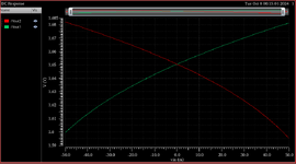
Of course, these voltages are not precise and can be though only as a first order estimate. That is why I have chosen V_icm=300mV to stay "safely" inside the estimated headroom. Moreover, as I wrote in the 3rd reply, Spectre finds a DC solution for a cellview version of the circuit and even plots the outputs. The main problem is that PM8 and PM10 which drains are the actual outputs of the amplifier are basically shorted to the drains of the upper PMOSes (please see the attachments with the op's for the nodes). Thereby I can not really expect any adequate gain performance.
I am also attaching the input file to the cellview testbench.
 

Attachments

  • cellview_input.txt
    32.1 KB · Views: 19
  • folded_cellview.png
    folded_cellview.png
    35.9 KB · Views: 24
  • Vout_diff.png
    Vout_diff.png
    35.5 KB · Views: 25
Doesn't converge all that cleanly here either... Using gpdk version 4.5. But, do get more convergence than you did.

Out of curiosity -- if you replace Width and Length with numerical values, ie., no parameters. Will it converge then? Just thinking if the excessive tabulation of ad/ad/pd/ps creates something odd.

Still doesn't explain the subcircuit thingie. It probably is something obvious staring at us...
Hi again, jjx 👋
I have just tried replacing variable width and length with an absolute values for each transistor - output log looks exactly the same.
I am using 4.6 version - i doubt that the model differs a lot.
As you said, there is something super obvious and simple... I believe we found the reason soon and will be really surprised how obvious the error is 🧐
 

LaTeX Commands Quick-Menu:

Part and Inventory Search

Welcome to EDABoard.com

Sponsor

Back
Top