Continue to Site

Welcome to EDAboard.com

Welcome to our site! EDAboard.com is an international Electronics Discussion Forum focused on EDA software, circuits, schematics, books, theory, papers, asic, pld, 8051, DSP, Network, RF, Analog Design, PCB, Service Manuals... and a whole lot more! To participate you need to register. Registration is free. Click here to register now.

Error Amp compensation - uc3843

Status
Not open for further replies.

cybercheater

Newbie level 6
Newbie level 6
Joined
Jan 9, 2010
Messages
11
Helped
0
Reputation
0
Reaction score
0
Trophy points
1,281
Location
Malaysia, Kelate
Activity points
1,357
hi..how to calculate value for ea compensation network?
freq is about 500khz, output voltage 300v

**broken link removed**

Rp, Cp, Ri, Rd, Cf, Rf
 

Attachments

  • Clipboard01.jpg
    Clipboard01.jpg
    32.7 KB · Views: 154
Last edited:

That's a pretty bizarre compensation network... When compensating these things, I usually stick to standard type II and type III networks. Here is an excellent white paper on compensation networks.
**broken link removed**

Note that these procedures are aimed at voltage mode converters. If you're using a current mode converter, then a type II converter should be plenty. If you are using voltage mode, and want to really optimize bandwidth, then you should go for a type III network.
 

That's a pretty bizarre compensation network...

Indeed..

http://www.datasheetcatalog.org/datasheet/stmicroelectronics/4298.pdf

It also does not help much when there is no explanation why or the reasoning behind it. Then again it is just a basic data sheet otherwise I've seen this one crop up in real life and it hurt my head as well. So much so that I ripped it out and put something more meaningful in. Still, I suppose, each to their own.

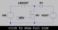
Let's say you have a boost converter operating with continuous inductor current. This might not be the most efficient or correct way of analysis things but it does show some of the salient points. The power stage is,


Operating Duty Cycle, Continuous Inductor Current

During switch on time, TON, the inductor is set through VIN. During switch off time, TOFF, it is reset through [VOUT - VIN]. The change in current through the device during each phase is,

dIset = TON.VIN/L

dIrset = TOFF.[VOUT - VIN]/L

Steady state with continuous inductor current the average does not change so,

dIset = dIrset

and therefore,

TON.VIN/L = TOFF.[VOUT - VIN]/L

Cancel L,

TON.VIN = TOFF.[VOUT - VIN]

Normalise to one second and TON becomes the operating duty cycle, D, with TOFF becoming [1 - D]. Substitute,

D.VIN = [1 - D].[VOUT - VIN]

Multiply out,

D.VIN = VOUT - VIN - D.VOUT + D.VIN

Rearrange a bit,

VOUT - VIN = D.VOUT

And a bit more,

D = [VOUT - VIN]/VOUT

It is the operating duty cycle for a boost converter with continuous inductor current.

Perturb The Duty Cycle

by a small amount, p.

D => [D + p]
[1 - D] => [1 - D - p]

The setting volt-seconds become,

Vset = [D + p].VIN

The setting volt-seconds become,

Vrset = [1 - D - p].[VIN - VOUT]

This results in a change of voltage across the inductor

dVL = [D + p].VIN - [1 - D - p].[VOUT - VIN]

Multiply out

dVL = D.VIN + p.VIN - VOUT + VIN + D.VOUT - D.VIN + p.VOUT -p.VIN

Some bits cancel

dVL = VIN - VOUT + D.VOUT + p.VOUT

We've already worked out the duty cycle D as being,

D = [VOUT - VIN]/VOUT

So substitute,

dVL = VIN - VOUT + [VOUT - VIN].VOUT/VOUT + p.VOUT
dVL = VIN - VOUT + VOUT - VIN + p.VOUT

Things disappear

dVL = p.VOUT

It's all algebra, sort of.

The change in voltage across the inductor results in a change in current though it. Given XL is the 'impedance' of the inductor then,

dIL = dVL/XL

dIL = p.VOUT/XL

dIL = -j.p.VOUT/2pi.f.L

The change in inductor current is 'sampled' at the output during the switch off time so, to begin with, the change in output current is,

dIOUT = [1 - D].dIL

but.... but... but....!!1! The perturbation, p, also acts to 'un-sample' the steady state inductor current delivered to the output so in fact,

dIOUT = [1 - D].dIL - p.IL

dIOUT = -j.p.[1 - D].VOUT/2pi.f.L - p.IL

Substitute for D again..

dIOUT = -j.p.[1 - [VOUT - VIN]/VOUT]].VOUT/2pi.f.L - p.IL

Fiddle about,

dIOUT = -j.p.[VOUT - VOUT + VIN]/2pi.f.L - p.IL
dIOUT = -j.p.VIN/2pi.f.L - p.IL

dIOUT = p.[-j.VIN/2pi.f.L - IL]

Rearrange, for the 'power circuit gain', control to output response, and the change in output current in response to the original perturbation, p, is..

dIOUT/p = -j.VIN/2pi.f.L - IL

This is the 'Right Half Plane Zero' and results from the perturbation 'un-sampling' the steady state inductor current. You ask for more but before you get it you get less.

Setting to unity gain and 'ignoring' -j then it lives at,

1 = VIN/2pi.frhpz.L - IL

IL = VIN/2pi.frhpz.L

frhpz = VIN/2pi.IL.L

In amplitude terms it behaves like a normal zero. Unfortunately instead of the phase going plus 90 degrees as you transition it the phase goes minus 90 degrees. There is no solution and you are forced to close your overall feedback loop at a lower frequency than that associated with it.

Now I may have made a mistake but, in the case of Power Factor Correction, given VIN will fall to zero then frhpz, according to the above, must do the same. If it is right then I might only assume that any loop applied does not have time to go and do unstable sillies before it enters stability again.

That's just me being sad and thinking about consequences.

Anyway. That's the method and that's the power circuit gain for a boost converter. You can also use a similar method to look at what flyback and indeed other circuits might do. It is part of building up blocks within the loop to add together before you apply your error amplifier.

I'll have to think about how 'peak' current mode control fits in with things so for the moment that is, not, a wrap.

Genome.
 

Here we go again...

dIOUT/p = -j.VIN/2pi.f.L - IL

Now we have to work out where the perturbation, p, came from. If this was 'voltage mode control' then it would be due to a comparison of the output of the voltage error amplifier to the modulator ramp,

p = dVvea/Vs

Where Vs would be the ramp amplitude, valley to peak. This of course is peak current mode control so we can't do that however there is a 'ramp' being used and that is the current upslope in the inductor converted to a voltage across the current sense resistor.

dILon/dT = VIN/L

dVRsns/dT = RSNS.VIN/L

What we don't know is its 'amplitude' but that can be fixed by taking the limit as being the converters switching frequency, Fsw,

dVRsns = RSNS.VIN/Fsw.L

So the perturbation becomes,

p = dVvea.Fsw.L/RSNS.VIN

Previously

dIOUT/p = -j.VIN/2pi.f.L - IL

So

dIOUT.RSNS.VIN/dVvea.Fsw.L = -j.VIN/2pi.f.L - IL

Rearrange

dIOUT/dVvea = Fsw.L[-j.VIN/2pi.f.L - IL]/RSNS.VIN
dIOUT/dVvea = -j.Fsw/2pi.f.RSNS - Fsw.L.IL/RSNS.VIN

dIOUT/dVvea = Fsw/RSNS . [-j/2pi.f - L.IL/VIN]

but... but... but... For the UC384X series there is a 2R/R divider on the output of the voltage error amplifier so the 'real' answer is,

dIOUT/dVvea = Fsw/3RSNS . [-j/2pi.f - L.IL/VIN]

So that gives the control to output response from the output of the voltage error amplifier to the current delivered to VOUT which will be the load.

I am making this up as I go along so it might be a flight of fantasy. Back later for a dive into LTSpice.

Genome.
 

Time for more,

dIOUT/dVvea = Fsw/3RSNS . [-j/2pi.f - L.IL/VIN]

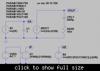
Can be modelled in LTSpice as,


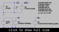
VVEA is going to be the output of the UC384X error amplifier and is applied to a voltage controlled voltage source with gain set to Fsw/3RSNS. The result is used by B1 and B2 to create the terms in [] above. C1 driven by B1 as a current source gives -j/2pi.f and B2 implements the second term. B3 does the final sum to get the output current.

There is a table of parameters top right which should explain themselves. IL in B2 is calculated as POUT/VIN..

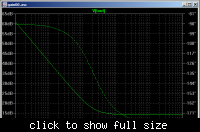
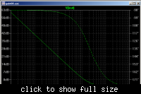
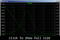
Running an AC analysis gives,


We get the expected 20dB/Decade roll-off with 90 degrees phase lag and then the zero.... but instead of the phase returning to zero itself it goes the other way resulting in an overall 180 degrees phase lag. It is the Right Half Plane Zero... RHPZ and, in analog terms, is something you can do little to nothing about other than avoid it.

In this case it is sitting at about 2.1KHz which is 'low' but then we are dealing with a high power circuit and steady state current in the inductor is large. This is actually taken from another thread where someone else may be having loop compensation problems so I thought I'd kind of combine the two. That might not be board etiquette but...

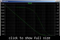
The above is set to 'worse' case. Maximum power with Minimum input voltage. The other possible operating points of interest might be,

Maximum Power Maximum Input Voltage,


Low Power [60W vs 600W] Maximum Input Voltage,


Low Power [60W vs 600w] Minimum Input Voltage,


In all cases the RHPZ moves out to higher frequencies and therefore becomes less of a concern. You would still have to design for the minimum. The other converter is required to give 600W out from a minimum input voltage of 18V. Some people are just hard.

The output capacitor for such a beast is going to suffer from high ripple currents. It is not as if the rest of the circuit won't be carrying heavy currents either. I have a 'basic' switching model set up for it that says the RMS ripple current is 13.75A so I'll go and hunt for a capacitor that might like that.

This won't be right...

https://www.farnell.com/datasheets/415501.pdf

Table 4] Page 9)


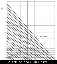
100V Frequency multiplier for ripple current 1.22 That brings things down to 11.27A. Let's say the product will be in continuous use for 2 years at 60C ambient. 17,520 hours. Indicated stress life, 105C/MaxIr, is 5000Hrs so I am looking for a lifetime multiplier at 60C of 3.5,


That lets me increase the rated ripple current by a factor of 1.9 so we are down to 5.93A...


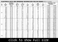
And I shall pick two 1500uF 30x40 59152E3. I think that the way the tabels have been labelled may be in error. Impedance > 10KHz is 85mR. Of course such values are subject to variations. Anyway, so that will be 3000uF bulk capacitance with an ESR of 43mR and we can slap that in the linear model...


I have converted B3 to a current source as BIOUT to drive the filter capacitor and its ESR with the result being VOUT...

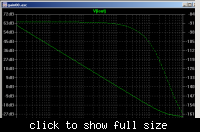
Setting 18V in and 600W out then running the AC analysis gives,


As expected a current source with a first order characteristic driving a capacitor becomes overall second order and down at low frequencies we get a slope of -40dB/Decade and a -180 degree phase shift. The ESR zero in the capacitor is at 1/2piCfiltResr or 1.23KHz so we might hope that the system would return to first order with a 90 degree phase lag.

It doesn't, although it tries, because the RHPZ wakes up in the same frequency range, 2.1KHz with two zeroes cancelling the two poles, taking the system first order, flat, and kills off the phase recovery of the ESR zero to hold things down at a -180 degree phase shift. :-(

To be continued..

Genome.
 

Actually.. I have to put my hands up and say some of the above is wrong, thus rendering things broken, because I've neglected to include the local feedback from the current limit comparator.

I shall try again later.

Genome.
 

Status
Not open for further replies.

Similar threads

Part and Inventory Search

Welcome to EDABoard.com

Sponsor

Back
Top