Continue to Site

Welcome to EDAboard.com

Welcome to our site! EDAboard.com is an international Electronics Discussion Forum focused on EDA software, circuits, schematics, books, theory, papers, asic, pld, 8051, DSP, Network, RF, Analog Design, PCB, Service Manuals... and a whole lot more! To participate you need to register. Registration is free. Click here to register now.

EMC measurement question help needed

Status
Not open for further replies.

Madbunny1

Member level 2
Member level 2
Joined
May 22, 2017
Messages
49
Helped
1
Reputation
2
Reaction score
1
Trophy points
8
Activity points
380
Hi all,

I would like to verify EMC emissions on my PCB board when it is functioning.

Can anyone answer my questions:
Can anyone please tell me which near field probe is better to use?
And how far the probe should be placed from my PCB?


Thanks
 

The best way is to use a calibrated broadband antenna 3 meters from the board (or whatever distance your regulatory agency wants it tested at) , and rotate the board all over the place.

There are near field probes, but they are in no way "calibrated" for accurate signal measuring.

These are kind of the industry standard:
**broken link removed**
 

The best way is to use a calibrated broadband antenna 3 meters from the board (or whatever distance your regulatory agency wants it tested at) , and rotate the board all over the place.
Thanks for the reply, So I can think Antenna is also same as like Near field probe. Is it right?

How will be the frequency ranges for automotive Standards?
 

there are hundreds of different types of "antennas", each with their own best uses. A "NEAR FIELD PROBE" can i suppose be thought of as an "antenna", although often they could better be described as a "magnetic loop", or as a "short capacitive coupler". The will NOT work well at any distance, so if you are trying to measure a field strength at 3 meters away, they will be useless. They ARE useful for pinpointing on a board or along a housing cover, exactly where the greatest amount of RF leakage is happening.

Ideally an engineering lab will have both Near Field probes and Calibrated gain antennas.

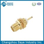
BTW, this can make a pretty good "near field probe" for microwave signals:

SMA probe.jpg

You can solder a wire into the center pin for lower frequencies.

Just remember that most spectrum analyzers do NOT like to have DC voltages input to them, so also use a microwave DC block if you are going to touch the probe to a board trace, like this one:

https://www.pasternack.com/50-ohm-sma-inner-dc-block-0.1-18-ghz-pe8210-p.aspx
 

there are hundreds of different types of "antennas", each with their own best uses. A "NEAR FIELD PROBE" can i suppose be thought of as an "antenna", although often they could better be described as a "magnetic loop", or as a "short capacitive coupler". The will NOT work well at any distance, so if you are trying to measure a field strength at 3 meters away, they will be useless. They ARE useful for pinpointing on a board or along a housing cover, exactly where the greatest amount of RF leakage is happening.

I have only H-field probe and E-field probe so I could only measure my PCB board with these probes. I tried of measuring EMI using H-field probe keeping 1 meter away to the board. Is this procedure I approached correct or not? Could you please tell me? And which probe can you suggest to use out of these two?

Thanks
 

Status
Not open for further replies.

Part and Inventory Search

Welcome to EDABoard.com

Sponsor

Back
Top