Continue to Site

Welcome to EDAboard.com

Welcome to our site! EDAboard.com is an international Electronics Discussion Forum focused on EDA software, circuits, schematics, books, theory, papers, asic, pld, 8051, DSP, Network, RF, Analog Design, PCB, Service Manuals... and a whole lot more! To participate you need to register. Registration is free. Click here to register now.

Embedded Linux on a PCB

Status
Not open for further replies.

40mpg

Newbie level 3
Newbie level 3
Joined
Feb 5, 2019
Messages
3
Helped
0
Reputation
0
Reaction score
0
Trophy points
1
Activity points
23
Hello all,

I am a student, i am trying to do something like the Olimex Maxi board. My board currently does not boot, i think it has something to do with the PSWITCH pin. If anyone knows what i am talking about that be great. But i am here to gather feedback on my schematic and board layout, thanx all.

they are on my google drive, a .sch and .brd file

IMX233 reference manual, if anyone is curious :https://www.nxp.com/docs/en/reference-manual/IMX23RM.pdf
 

Attachments

  • IMX23.zip
    129.5 KB · Views: 138

You did not specify in which CAD your board was made, but even if you said it, it would not be sure that everyone have the program, so you will surely have a best chance to get replied if you show here the images in browser viewable formats, such as GIF, PNG, etc ...
 

Hello, sorry, This is drawn in EAGLE.
 

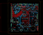
Adding an image, a png file of my board

RevB.png

[Found at: drive. google. com /open ?id =1xj3Y4Ttd CBcqQv5tRQd5S i16MxRFQnqy ]
 
Last edited by a moderator:

Some details may be problematic, such as the proximity of tracks on the component side, near of the pins of the connectors, which are not centralized between pins, but aligned to only one of the pins; I particularly prefer route on the bottom side, as this way I can remove any excess welds on the track. I would bet you have used the auto-route feature, which do not work well when design rules are not properly configured.

Another thing that caught attention was the reset button pointed to the inner side of the board, which increases the chance of when being pressed, bumping your finger into any component, ripping it off, or injecting static electricity into the board.

Also notable is the lack of mounting holes for fixing the board, or space in the laterals for fastening it in guides.

In addition, the crystal is too far away from the microcontroller, which increase the chance of issues related to EMI.

The J-TAG connector is placed too far from the microcontroller.

Seriously speaking, I would recommend review this layout before manufacturing the PCB.
 

Status
Not open for further replies.

Part and Inventory Search

Welcome to EDABoard.com

Sponsor

Back
Top