Continue to Site

Welcome to EDAboard.com

Welcome to our site! EDAboard.com is an international Electronics Discussion Forum focused on EDA software, circuits, schematics, books, theory, papers, asic, pld, 8051, DSP, Network, RF, Analog Design, PCB, Service Manuals... and a whole lot more! To participate you need to register. Registration is free. Click here to register now.

[SOLVED] EM simulation for the large system

Status
Not open for further replies.

anh56789

Junior Member level 1
Joined
Jul 27, 2023
Messages
19
Helped
0
Reputation
0
Reaction score
0
Trophy points
1
Activity points
202
Hi everyone,

I'm working on my thesis about a beamformer system using CMOS 65nm technology. I am using the EM simulator from ADS software with the Momentum microwave engine. However, my EM layout is quite large, and the calculated mesh is extremely detailed, making it difficult to simulate the full system. As a result, I have to divide the system into smaller parts and simulate each part individually.

I have attached a snapshot of my setup, which includes an amplifier and a 1-to-2 Wilkinson power divider. I have separated them and placed pins to facilitate EM simulations for each circuit. Additionally, I have placed ground pins at the boundaries of each circuit to connect to the ground plane.

I have a couple of questions:
  1. Is breaking the circuit into smaller pieces a valid approach? I believe this method may work at lower frequencies, but I am concerned that higher frequencies could lead to coupling effects that might create discrepancies. Since the layout includes a large ground plane, the mesh for this ground plane is also substantial, complicating EM simulations. Do you know of any methods that could help me address this issue?
  2. Regarding the ground pins around these circuits, I have noticed that the number of pins can significantly affect the simulation results. I am confused about why this happens. Can you provide any insights on this?
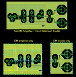
Any insights on these issues would be greatly appreciated. Thank you so much!
 

Attachments

  • test2.jpg
    test2.jpg
    295.1 KB · Views: 38

"Divide and conquer" is a valid approach. This is a good strategy for MoM simulations because memory scales with the square of number of subsections. In your layout, I don't see much risk for cross coupling between pieces.

However, your placement of ground pins is not valid. These redundant closely spaced ports which almost identical voltages can lead to matrix singularities and invalid results. I understand why you tried this, but it's causing issues. From a physical viewpoint, there is no need to have all those pins in places where "nothing happens". Current flow is mostly on the edges, and the really important ground plane ports are near the signal port, which seem to be missing in your screenshot.

I would reduce the ground plane pins to a single ground pin left and right from the input and output, with manually controlled port width of a few microns. When you run that simulation, you will also see if there is any resonance in the remaining ground plane that would require more ports to connect other ground plane pieces.

Regarding mesh density, ADS allows to set different mesh density for different layers, and even for different polygons. You could try to simulate the ground planes as thin metal (sheet) and only the signal traces as thick metal. This will save a lot of mesh cells, and thick metal model has very small effect for these planes that are far away from the conductors. Just enable edge mesh for the ground polygons, but not thick metal.
--- Updated ---

For an example of agressive partitioning, you might have a look here:


This work was done with the Sonnet MoM solver, which has more accurate port calibration than Momentum, but it gives an idea how extreme the partitioning could be without excessive error in results.
 
Last edited:
Thank you for your quick response!
When you run that simulation, you will also see if there is any resonance in the remaining ground plane that would require more ports to connect other ground plane pieces.
Could you explain more on this, I don't understand your point here and How can I see the resonance in the ground plane?
I would reduce the ground plane pins to a single ground pin left and right from the input and output, with manually controlled port width of a few microns
If I only use one ground pin for input/output signal, I know that the ground pin must be near the signal pin, but for example, in my layout, I can place the pin on the ground above the signal pin or the ground below it, where should I place the pin? we see that if we use the signal path as the boundary line, we will have two separated ground planes and they may have different impedances so that the results would be different from each other, am I right?
 

I mean that if you simulate your layout, you can check current density calculated by Momentum and see where current is flowing. You will notice that there is no current flow on those remote ground areas, far away from the signal path. Placing many ports there has no benefit, and creates the risk of numerical issues if those ports are "almost identical" with just some micron of copper between them. That's why I strongly recommend to place only ports that matter for current flow.

To see current density, you must enable that in emSetup > Output plan, and define what frequencies should be saved to disk. For an initial analysis, you can choose "all generated frequencies".

For a coplanar ground, see the screenshot below, this is a sketch how I model these cases. The port size L for the grounds is an estimate, I usually make that equal to the line or gap width, or maybe a little larger. Don't make those ports too wide.

edgeport.png
 
Status
Not open for further replies.

Part and Inventory Search

Welcome to EDABoard.com

Sponsor

Back
Top