Continue to Site

Welcome to EDAboard.com

Welcome to our site! EDAboard.com is an international Electronics Discussion Forum focused on EDA software, circuits, schematics, books, theory, papers, asic, pld, 8051, DSP, Network, RF, Analog Design, PCB, Service Manuals... and a whole lot more! To participate you need to register. Registration is free. Click here to register now.

Electronic DC Voltmeter circuit

Status
Not open for further replies.

MSAKARIM

Full Member level 3
Full Member level 3
Joined
Jun 2, 2015
Messages
154
Helped
1
Reputation
2
Reaction score
4
Trophy points
1,298
Activity points
2,528
This circuit is a DC voltmeter, I want to know why the two transistors are arranged in this manner?
Is Q1 is common emitter and Q2 is common collector?
why suppely E connected like this?
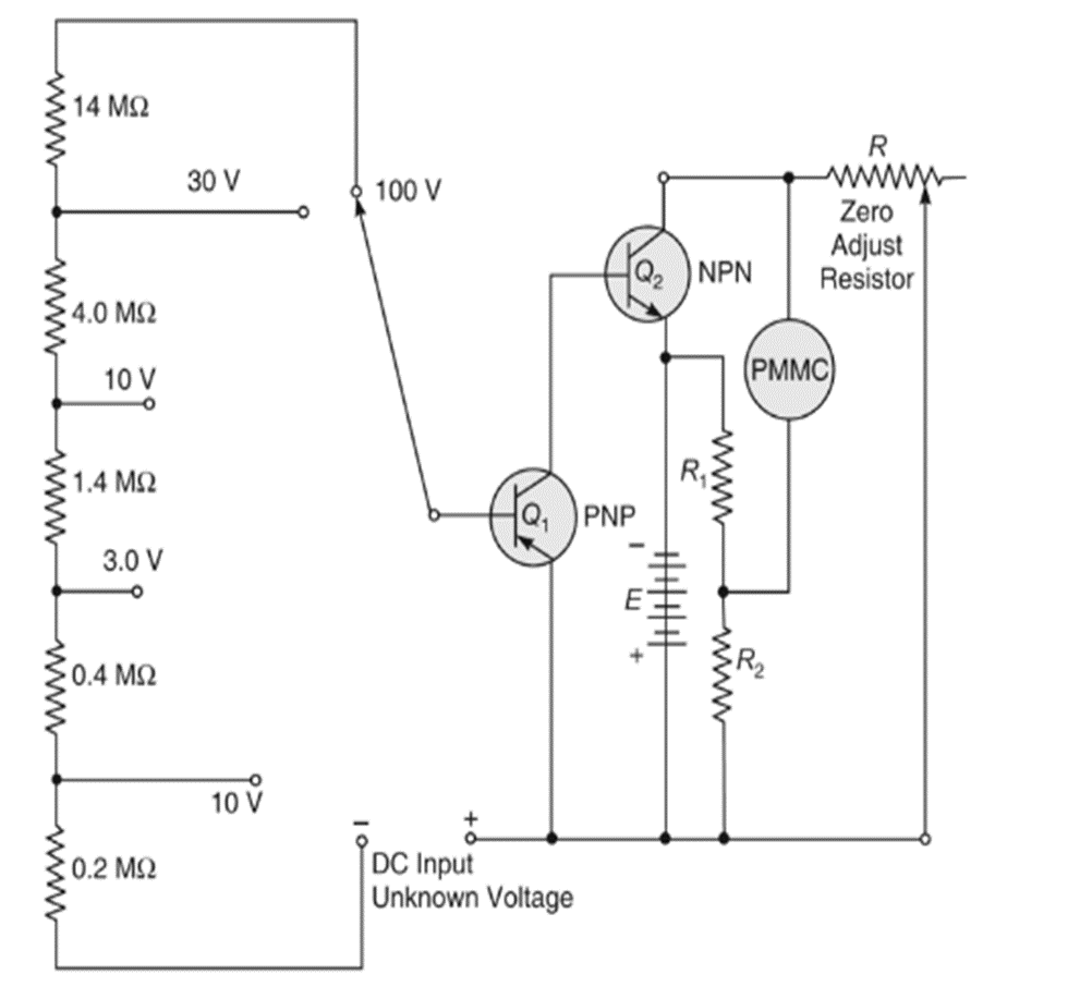
1697725113766.png
 

Hi,

The transistors try to amplify the measurement current (input voltage / resistor).

why suppely E connected like this?
Whats wrong with it?
How do you you expect it to be wired?

******

But it´s a really bad circuit. It may be from 1960 to 1970. So really outdated.
It´s not accurate at all and it drifts a lot with temperature.
--> The displayed value is not reliable.

Klaus
 

Another possible explanation is that the schematic has errors and the real circuit is different, if it's at all the schematic of a real instrument.

Range resistors seem to fit a standard 50 uA moving coil instrument (20 kOhm/V), it won't use amplifier transistors.

I rather guess that the schematic is a mixed-up combination of resistor measurement circuit, regular voltage input. Transistors may either provide overvoltage clamp or a different function.
 

Anecdotal:
I recall drawing power from a DMM battery and noticed as in this circuit that Vbat+ and Vin+ were common.
But this schematic looks flawed with hFE dependancy. I wonder if PNP is installed in reverse to reduce the hFE to near 1.

2009 was the earliest similar match of this schematic, on www.Circuitstoday.comhttp://www.circuitstoday.com/dc-voltmeters
by Author jojo

I agree with FVM Frank's description and the design is flawed.
Always check who created the design and look for missing information as a clue to an unfinished drawing.
 

Q1 Q2 are arranged as a sziklai pair. It's made from NPN and PNP and operates similar to a Darlington pair. Both types have an advantage of high gain yet draw tiny bias current through those high-ohm resistors.
 

Q1 Q2 are arranged as a sziklai pair. It's made from NPN and PNP and operates similar to a Darlington pair. Both types have an advantage of high gain yet draw tiny bias current through those high-ohm resistors.
For this design to be accurate with unknown hFE it is not suitable. The bias is wrong and will not work with excess offset and gain introduced.
 

Status
Not open for further replies.

Part and Inventory Search

Welcome to EDABoard.com

Sponsor

Back
Top