Continue to Site

Welcome to EDAboard.com

Welcome to our site! EDAboard.com is an international Electronics Discussion Forum focused on EDA software, circuits, schematics, books, theory, papers, asic, pld, 8051, DSP, Network, RF, Analog Design, PCB, Service Manuals... and a whole lot more! To participate you need to register. Registration is free. Click here to register now.

Effect of the bonding wire on power supply pin.

Mvitale

Newbie
Newbie level 3
Joined
May 31, 2024
Messages
4
Helped
0
Reputation
0
Reaction score
0
Trophy points
1
Activity points
44
I'm a PhD student and I'm dealing with the design of an ADC pipeline 10 bit, 50 Msps:
1721295212241.png

four 2.5bit stage and last 2 bit Flash.

This is the 2.5bit stage, The OTA is a pseudodifferential ring Amp.:
1721296036188.png


In order to take in to account the effect of the parasitic capacitances and inductances of the bonding wire on the power supply, I implemented a simple model showed below:
1721294247283.png

vdd and gnd power the ADC circuit.


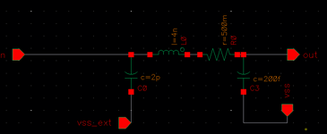
Inside the box there is the following circuit:
1721294401114-png.192452

where vss_ext is the external ground, and vss is the internal ground of the circuit.
It is a common model that I observe in many paper.

This is the residium of the first stage with "ideal" power supply without the PAD effect.
1721295092322.png


When I include the bonding wire circuit (that I showed up) the residium start to oscillate:
1721295704999.png

This happened for all the stages.


The problem is the inductances on the power supply:
1721295861134.png

Indeed, if I reduce the nominal value, the oscillation decrease.


The only way I've found to reduce oscillations is to put multiple bonding wires in parallel, implementing the following model:
1721296473513.png

But I dont know if it is feasible this solution.
Do you have any other ideas regarding this problem?


Really Sorry if I wasn't very clear in describing the problem, if necessary I'm available to answer your questions.
 

Attachments

  • 1721294401114.png
    1721294401114.png
    14.9 KB · Views: 165
If you can follow supply activity down to where the behavior starts then maybe local decoupling, filtering at the block level on chip can tamp it down.

Be sure you are not (over)reacting to some "tank artifacts" of the lumped LCR (and what about the mutuals? Think of the children...).
Might substitute a bond wire subcircuit with all the elements /8 and 8X of them, move the tank tone by 3 octaves and assess. This might tell you more about where / why and about effectiveness of specific filtering measures.
 
Another point, I see 4nH on the bond wire inductor which
by my rule of thumb is about a 4mm bond. That's kinda
long, maybe sane for a corner but look at I/O ring & floor
plan to see if you can do things like put power on the
middle of the chip edge for shortest bond and internal
leadframe / trace length, interdigitate bond-posts for vdd
and vss for some free mutual-C as you head in to the guts,
etc.

Although this is not any kind of a barn-burner part, package co-
design is often a thing and not always about speed or current.

Re the "oscillation" - is it truly oscillatory, or is it a "memmory
effect" that is only bistable & clocked with sub-residue returning
as an intial condition for next cycle? Check this by lowering the
clock rate significantly (though not so significantly that it bleeds
out any sampled data accuracy) and see if more settling time
cuts next-sample error.
First of all, I would like to thanks you for your answers!
Now that you point out, I lowered the clock rate from 100 MHz to the current 50 MHz and the "oscillations" have reduced.
Maybe it's a "memory effect problem". How can I deal with that?
 
Is it the source impedance of voltage mode DAC logic from a passive RLC step response with Q? Then Zo/Rs is your response. Can you convert to CML?
--- Updated ---

ESL can vary by log (l/w) ratio might be 0.5nH/mm on short lengths
 
Last edited:

LaTeX Commands Quick-Menu:

Similar threads

Part and Inventory Search

Welcome to EDABoard.com

Sponsor

Back
Top