analogman
Junior Member level 1

Now I design dynamic comparator for pipeline ADC.
But there are some problems.
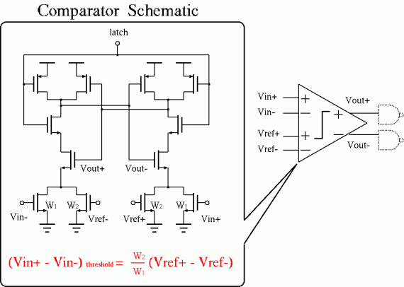
This is my design parameter.
Vdd = 3.3V (CM = 1.65V)
Vref+ = 1.9 V
Vref- = 1.4 V
Vin+ - Vin- ; ramp signal from -3.3V to 3.3V
1. This comparater generates 1/4Vref threshold voltage if I design W2/W1=0.25.
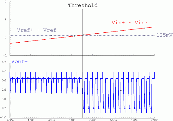
Simulation with only compater was well done.
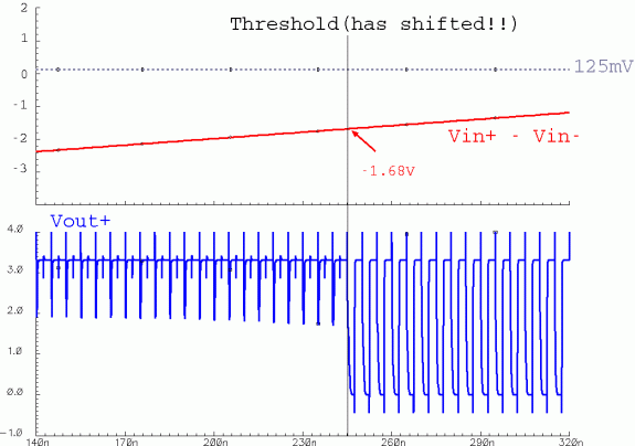
But I put NAND gate at the output node of comparater, the threshold
voltage has shifted!! I can't find the reason at all so it troubles me...
Anyone tells me about the reason please.
【Only comparator simulation】
【with NAND gate simulation】
2. I use this comparater directly linking to MDAC. But some papers use S/H
configuration. I don't know which is correct...
I think to use S/H configuration will become large input capacitance.
Sorry, for my poor english and explanation.
I want your help!
But there are some problems.

This is my design parameter.
Vdd = 3.3V (CM = 1.65V)
Vref+ = 1.9 V
Vref- = 1.4 V
Vin+ - Vin- ; ramp signal from -3.3V to 3.3V
1. This comparater generates 1/4Vref threshold voltage if I design W2/W1=0.25.
Simulation with only compater was well done.
But I put NAND gate at the output node of comparater, the threshold
voltage has shifted!! I can't find the reason at all so it troubles me...
Anyone tells me about the reason please.
【Only comparator simulation】

【with NAND gate simulation】

2. I use this comparater directly linking to MDAC. But some papers use S/H
configuration. I don't know which is correct...
I think to use S/H configuration will become large input capacitance.
Sorry, for my poor english and explanation.
I want your help!


