Continue to Site

Welcome to EDAboard.com

Welcome to our site! EDAboard.com is an international Electronics Discussion Forum focused on EDA software, circuits, schematics, books, theory, papers, asic, pld, 8051, DSP, Network, RF, Analog Design, PCB, Service Manuals... and a whole lot more! To participate you need to register. Registration is free. Click here to register now.

Duty cycle vs. load in off-line forward converter

Status
Not open for further replies.

kekon

Full Member level 3
Full Member level 3
Joined
Sep 19, 2002
Messages
155
Helped
5
Reputation
10
Reaction score
3
Trophy points
1,298
Location
Poland, Białystok
Activity points
1,493
I've built several off-line forward converters so far. However i always face the problem how duty cycle depends on connected load. Most of my designs use two transistor topology so theoretical maximum duty cycle is limited to 50% (in practice i always use about 40..45%).
For example, a 320W forward converter (80V, 4A) has 43% duty cycle at lowest input voltage and full load. When 2A is drawn (half load) the duty cycle in not 2x lower (about 21 %) but it stays at about 35% so it seems that duty cycle relationship vs load is not linear. I want to find mathematical formula to calculate it. Did someone of you have similar problem ?
 
Last edited:

for 2TFC

Vout/Vin = ND

where N = ns/np

Unless you are in discontinuous mode and then you use power in = power out/efficincy and then work it like that.
 

As grizedale explained, the duty cycle should only depend on the voltage ratio. There are however several points against this ideal behavior. One deviation is caused by windings resistance and leakage inductance and respective voltage drops. The other is due to part of the magnetization current recovered to the secondary (if a two way output rectifier is used).
 

Thanks for all suggestions. I wanted to know how to solve my problem because i'm designing new forward converter which will have adjusted output voltage 50..80V, 4A. It will also include PFC circuit that needs external voltage supply to work (about 18V). At the beginning i thought about adding slave power supply to provide 18V for the PFC. But it requires to include another transformer which i would like to avoid. It would be nice to add an extra winding to the main transformer to obtain 18V. Obviously, the extra winding would provide voltage which value would depend on the current and voltage on the adjusted 50..80V output. At the lowest load and voltage (say 50V, 100mA) the extra winding would generate very low voltage which value is unknown. That's why i wanted to know how duty cycle changes with main output load and it would be helpful to calculate the voltage at the extra winding for PFC regulator.
 

Tracking of multiple output voltages with varying loads is always difficult, but effectively impossible with forward converters and discontinuous current in the output inductors. You'll need special means like coupled inductors. In addition, it's not clear from your post, if your design includes output inductors at all.

Of course, the output voltages can be calculated if you put in all parameters, but calculation possibly won't help you for a multiple output design.
 
My design will not have coupled inductors. It seems it will be better to use additional slave power supply...

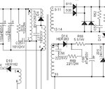
I also have schematic diagram of MeanWell 320W power supply as well as its transformer construction details. They use one-transistor topology and additional two auxiliary windings. One is used to supply ML4800 chip and one for a cooling fan. I wondered why they didn't use two-transistor topology. It think it's due to manufacturing costs. I'm not allowed to post the whole schematic of MeanWell power supply but only a part of it. I think C25 and R18 are used to supress voltage spike generated as a result of leakage inductance. I wonder what is the purpose of C7 capacitor ? (10 nF/2kV)
 

Attachments

  • trafo.jpg
    trafo.jpg
    55.9 KB · Views: 84

I wondered why they didn't use two-transistor topology.
It's rarely used for general purpose SMPS. More because of it's disadvantages (limited duty cycle respectively voltage ratio) than it's costs, I suppose.

You see, that the auxilary secondary output has no inductor but a voltage limiting zener diode. It indicates, that the designer didn't even try to achieve tracking of output voltages. I guess, it's intended as a fan supply.

I assume, that the SMPS is specified for current output range from zero, thus discontinuous mode will be part of the operation range. At least in DCM, duty cyle won't represent the voltage ratio and PWM gain increases.
 
  • Like
Reactions: kekon

    kekon

    Points: 2
    Helpful Answer Positive Rating
You see, that the auxilary secondary output has no inductor but a voltage limiting zener diode. It indicates, that the designer didn't even try to achieve tracking of output voltages. I guess, it's intended as a fan supply.

Yes, it's used as a fan supply.
The only thing i don't know yet is the purpose of C7 capacitor.
 

Status
Not open for further replies.

Similar threads

Part and Inventory Search

Welcome to EDABoard.com

Sponsor

Back
Top