with2ls
Junior Member level 3

I'm looking into a bidirectional converter design for charging a battery bank when a mains connection is available, and operating as an inverter when mains is not available.
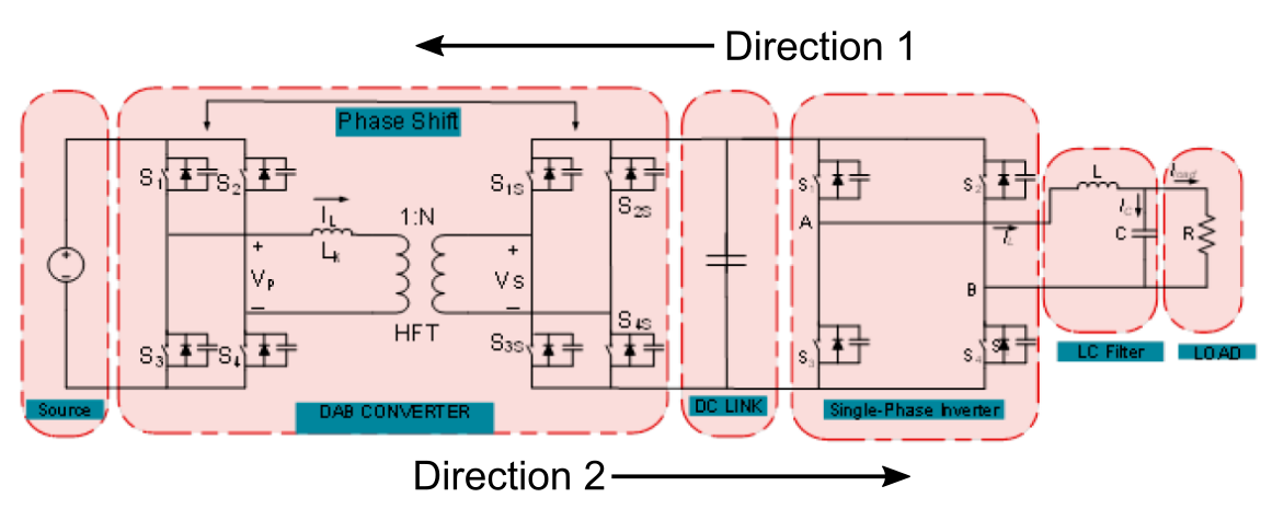
The design is similar to the following picture:

The operation in Direction 1 (as a battery charger) is clear to me:
1. "Load" is replaced with the mains connection.
2. "LC Filter" and "Single Phase Inverter" operate as a Boost PFC, generating a DC voltage (let's say 380V).
3. DAB operates to transfer power from the ~380V to the battery using a number of modulation options (phase shift modulation for example).
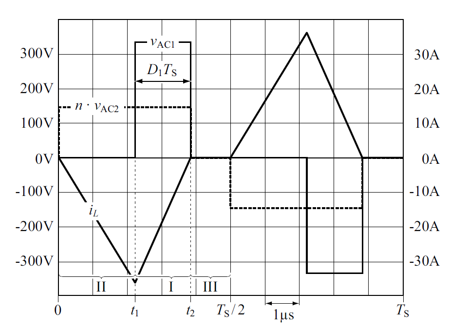
Direction 2 (as an inverter) is where I am struggling. Most of the DAB papers I have read imply that the DAB is used to transfer power from one source to another, which render pretty plots like the following:

but in this case, I need to actually generate the high voltage side starting at 0V.
1. Is there a special modulating scheme for doing this?
2. In Direction 2, is the output voltage limited by the input voltage * the turns ratio of the transformer? Or can it operate as a boost using the leakage inductor?
3. Assuming it can operate as a boost to output ~380V, is it then acceptable to switch to a normal modulate scheme (phase shift or triangle)?
Any advice is much appreciated.
The design is similar to the following picture:
The operation in Direction 1 (as a battery charger) is clear to me:
1. "Load" is replaced with the mains connection.
2. "LC Filter" and "Single Phase Inverter" operate as a Boost PFC, generating a DC voltage (let's say 380V).
3. DAB operates to transfer power from the ~380V to the battery using a number of modulation options (phase shift modulation for example).
Direction 2 (as an inverter) is where I am struggling. Most of the DAB papers I have read imply that the DAB is used to transfer power from one source to another, which render pretty plots like the following:
but in this case, I need to actually generate the high voltage side starting at 0V.
1. Is there a special modulating scheme for doing this?
2. In Direction 2, is the output voltage limited by the input voltage * the turns ratio of the transformer? Or can it operate as a boost using the leakage inductor?
3. Assuming it can operate as a boost to output ~380V, is it then acceptable to switch to a normal modulate scheme (phase shift or triangle)?
Any advice is much appreciated.