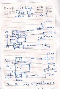
driving full bridge using ir2110
- Thread starter praki
- Start date
- Status
- Not open for further replies.
alexan_e
Administrator

Yes this is the basic connection circuit for the chip, check the following application note
www.irf.com/technical-info/appnotes/an-978.pdf
Alex
www.irf.com/technical-info/appnotes/an-978.pdf
Alex
Orson Cart
Advanced Member level 3

- Joined
- Jun 18, 2009
- Messages
- 798
- Helped
- 347
- Reputation
- 1,146
- Reaction score
- 558
- Trophy points
- 1,373
- Location
- New Zealand
- Activity points
- 5,973
Depending on the min PWM of the low side, 220nF-470nF will be OK for the bootstrap caps, 10 ohm for the gate drive res, diodes = schottky 45V 1A, 1uF for the de-coupling caps in the chip.
Regards, Orson Cart.
Regards, Orson Cart.
alexan_e
Administrator

Vb is the generated bootstrap voltage , if you leave it open the high side mosfet can't work.
The Vcc is the power supply of the logic control circuit, this controls the operation of the output stage,
why would you remove that?
Alex
The Vcc is the power supply of the logic control circuit, this controls the operation of the output stage,
why would you remove that?
Alex
alexan_e
Administrator
But i already did....
The Vb is connected to the bootstrap diode and capacitor and is the bootstap voltage input,
then this voltage is used internally for the mosfet driver stage,
if this voltage is not connected then the high side mosfet driver can't drive the mosfet.
The Vdd and Vss are the positive supply and ground of the digital control circuit of the chip,
if you don't provide these then the output stage can't be controlled.
Alex
Last edited:
Orson Cart
Advanced Member level 3
- Joined
- Jun 18, 2009
- Messages
- 798
- Helped
- 347
- Reputation
- 1,146
- Reaction score
- 558
- Trophy points
- 1,373
- Location
- New Zealand
- Activity points
- 5,973
Vcc has to go to +12V referenced to 0V, when the bottom mosfet turns on, Vb gets its energy from Vcc via the diode.
Regards, Orson Cart.
Regards, Orson Cart.
alexan_e
Administrator
Yes sorry, Vdd is power supply of the digital control circuit ,
Vcc is the positive supply of the output stage.
I'm used to having Vcc as power supply in digital ic and i have mixed them up.
Alex
Vcc is the positive supply of the output stage.
I'm used to having Vcc as power supply in digital ic and i have mixed them up.
Alex
- Status
- Not open for further replies.
Similar threads
-
Full Bridge is Dead....Phase Shift Full Bridge replaces it?
- Started by cupoftea
- Replies: 1
-
-
-
Need Opinions on the my output Current waveform of Phase Shifted Full bridge
- Started by Pulasthi_Perera
- Replies: 7
-


