Continue to Site

Welcome to EDAboard.com

Welcome to our site! EDAboard.com is an international Electronics Discussion Forum focused on EDA software, circuits, schematics, books, theory, papers, asic, pld, 8051, DSP, Network, RF, Analog Design, PCB, Service Manuals... and a whole lot more! To participate you need to register. Registration is free. Click here to register now.

Driving 7 SEGMENT display

Status
Not open for further replies.

venkates2218

Full Member level 6
Full Member level 6
Joined
Sep 30, 2016
Messages
354
Helped
1
Reputation
2
Reaction score
1
Trophy points
1,298
Activity points
4,306
Code:
#include "xc.h"
#define	XTAL_FREQ	20MHZ		/* Crystal frequency in MHz */
#include "delay.h"
#include "eeprom.h"

// CONFIG1H
#pragma config OSC = HS         // Oscillator Selection bits (HS oscillator)
#pragma config FCMEN = OFF      // Fail-Safe Clock Monitor Enable bit (Fail-Safe Clock Monitor disabled)
#pragma config IESO = OFF       // Internal/External Oscillator Switchover bit (Oscillator Switchover mode disabled)

// CONFIG2L
#pragma config PWRT = ON       // Power-up Timer Enable bit (PWRT disabled)
#pragma config BOREN = OFF      // Brown-out Reset Enable bits (Brown-out Reset disabled in hardware and software)
#pragma config BORV = 3         // Brown Out Reset Voltage bits (Minimum setting)

// CONFIG2H
#pragma config WDT = OFF        // Watchdog Timer Enable bit (WDT disabled (control is placed on the SWDTEN bit))
#pragma config WDTPS = 32768    // Watchdog Timer Postscale Select bits (1:32768)

// CONFIG3H
#pragma config CCP2MX = PORTC   // CCP2 MUX bit (CCP2 input/output is multiplexed with RC1)
#pragma config PBADEN = OFF     // PORTB A/D Enable bit (PORTB<4:0> pins are configured as digital I/O on Reset)
#pragma config LPT1OSC = OFF    // Low-Power Timer1 Oscillator Enable bit (Timer1 configured for higher power operation)
#pragma config MCLRE = ON       // MCLR Pin Enable bit (MCLR pin enabled; RE3 input pin disabled)

// CONFIG4L
#pragma config STVREN = OFF      // Stack Full/Underflow Reset Enable bit (Stack full/underflow will cause Reset)
#pragma config LVP = OFF        // Single-Supply ICSP Enable bit (Single-Supply ICSP disabled)
#pragma config XINST = OFF      // Extended Instruction Set Enable bit (Instruction set extension and Indexed Addressing mode disabled (Legacy mode))

// CONFIG5L
#pragma config CP0 = OFF        // Code Protection bit (Block 0 (000800-001FFFh) not code-protected)
#pragma config CP1 = OFF        // Code Protection bit (Block 1 (002000-003FFFh) not code-protected)
#pragma config CP2 = OFF        // Code Protection bit (Block 2 (004000-005FFFh) not code-protected)
#pragma config CP3 = OFF        // Code Protection bit (Block 3 (006000-007FFFh) not code-protected)

// CONFIG5H
#pragma config CPB = OFF        // Boot Block Code Protection bit (Boot block (000000-0007FFh) not code-protected)
#pragma config CPD = OFF        // Data EEPROM Code Protection bit (Data EEPROM code-protected)

// CONFIG6L
#pragma config WRT0 = OFF       // Write Protection bit (Block 0 (000800-001FFFh) not write-protected)
#pragma config WRT1 = OFF       // Write Protection bit (Block 1 (002000-003FFFh) not write-protected)
#pragma config WRT2 = OFF       // Write Protection bit (Block 2 (004000-005FFFh) not write-protected)
#pragma config WRT3 = OFF       // Write Protection bit (Block 3 (006000-007FFFh) not write-protected)

// CONFIG6H
#pragma config WRTC = OFF       // Configuration Register Write Protection bit (Configuration registers (300000-3000FFh) not write-protected)
#pragma config WRTB = OFF       // Boot Block Write Protection bit (Boot block (000000-0007FFh) not write-protected)
#pragma config WRTD = OFF       // Data EEPROM Write Protection bit (Data EEPROM not write-protected)

// CONFIG7L
#pragma config EBTR0 = OFF      // Table Read Protection bit (Block 0 (000800-001FFFh) not protected from table reads executed in other blocks)
#pragma config EBTR1 = OFF      // Table Read Protection bit (Block 1 (002000-003FFFh) not protected from table reads executed in other blocks)
#pragma config EBTR2 = OFF      // Table Read Protection bit (Block 2 (004000-005FFFh) not protected from table reads executed in other blocks)
#pragma config EBTR3 = OFF      // Table Read Protection bit (Block 3 (006000-007FFFh) not protected from table reads executed in other blocks)

// CONFIG7H
#pragma config EBTRB = OFF      // Boot Block Table Read Protection bit (Boot block (000000-0007FFh) not protected from table reads executed in other blocks)


#define zero 0X40
#define one 0Xf9
#define two 0X24
#define three 0X30
#define four 0X19
#define five 0X12
#define six 0X02
#define seven 0XF8
#define eight 0X00
#define nine 0X10


#define segment1 PORTDbits.RD2
#define segment2 PORTDbits.RD3
#define segment3 PORTDbits.RD4
#define segment4 PORTDbits.RD5

int first_digit;
int tm1_change_timer, run_digit;
int temp1_counter, temp2_counter, temp3_counter, temp4_counter, temp5_counter, temp6_counter;

void one_display() {//1st digit
    switch (first_digit) {
        case 0:
            PORTB = zero;
            break;
        case 1:
            PORTB = one;
            break;
        case 2:
            PORTB = two;
            break;
        case 3:
            PORTB = three;
            break;
        case 4:
            PORTB = four;
            break;
        case 5:
            PORTB = five;
            break;
        case 6:
            PORTB = six;
            break;
        case 7:
            PORTB = seven;
            break;
        case 8:
            PORTB = eight;
            break;
        case 9:
            PORTB = nine;
            break;
        default:
            PORTB = zero;
            break;
    }
}

void System_init(void) {

    TRISA = 0b00000000;
    PORTA = 0b00000000;

    ADCON1 = 0XFF;
    CMCON = 0X07;

    TRISB = 0b00000000;
    PORTB = 0b11111111;

    TRISC = 0b00000000;
    PORTC = 0b11111111;

    TRISD = 0b00000000;
    PORTD = 0b11111111;

    TRISE = 0b00000111;
    PORTE = 0b00000111;
}

/**************************************************************
                    Main Program
 **************************************************************/


void main(void) {

    System_init();
    ee_init(); //EEPROM initialize


    while (1) {
        run_digit++;
        DelayMs(100);

        temp1_counter = run_digit / 1000;
        temp2_counter = run_digit % 1000;

        temp3_counter = temp2_counter / 100;
        temp4_counter = temp2_counter % 100;

        temp5_counter = temp4_counter / 10;
        temp6_counter = temp4_counter % 10;

        segment1 = 0;
        segment2 = 1;
        segment3 = 1;
        segment4 = 1;
        first_digit = temp1_counter;
        one_display();
        DelayMs(1);

        segment1 = 1;
        segment2 = 0;
        segment3 = 1;
        segment4 = 1;

        first_digit = temp3_counter;
        one_display();
        DelayMs(1);

        segment1 = 1;
        segment2 = 1;
        segment3 = 0;
        segment4 = 1;

        first_digit = temp5_counter;
        one_display();
        DelayMs(1);

        segment1 = 1;
        segment2 = 1;
        segment3 = 1;
        segment4 = 0;

        first_digit = temp6_counter;
        one_display();
        DelayMs(1);

        ee_write(1, 1);
        ee_write(2, 2);
        ee_write(3, 3);
    }

}

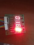
For displaying the values tried to use 7 SEGMENT display instead of LCD.When tried to display the value,first 3 digit are not showing properly it blinking...
I bought the 7 SEGMENT display from online its common anode....
Connected the display board directly to pic controller on PORTB and PORTD.
I have to store the datas in EEPROM,so I tired with simple values...
Like EEPROM operation,I have to do lot of operations,while executing the display will not show the correctly

I dono how to how to drive the display.Please help to solve this issue
7segment.jpg
 

You seem to have the concept of digits and segments crossed over. When we say 'digit' we mean the whole of the number on one 7-segment display and for 'segment' we mean the individual bars that make up the shape of the digit.

Your code is horribly inefficient but the basic problem is how long each digit (segment in your wording) is turned on for. Remember that only one digit is active at a time and the others are turned off. It is the human eye persistence of vision that makes it look as though all the digits are being displayed continuously. Because you are using delays "DelayMs(1);" between digits and "DelayMs(100);" at the start of each sequence, as well as all the time taken to store in the EE memory and do the calculations, the time before the first digit is updated is more than 100 times longer than the others.

The solution is to remove the switch/case section completely and store the segment values in an array, that replaces the whole of your "one_display()" routine with a single line and lets you remove all the #defines for each number. When the values are in an array all you have to do is select them with the array index.

To overcome the problem of digit timing, use a timer interrupt. This is very simple, just program one of the timers so it generates an interrupt every millisecond or so then use the interrupt routine to advance to displaying the next digit. That gives priority to updating the display so it looks good while leaving the calculations and EE storage to the main part of the program where the timing isn't critical.

Brian.
 
Hai i'm using timer 0 interrupt for displaying the value and timer 2 for other purpose...Is it correct to use both timers for different operation..?
 

Hi,

No, your code doesn't show any timer interrupt.
****

Why don't you look how others did the multiplexing?
There are a lot of discussions with code...

Klaus
 

In fact it shows no interrupts or references to any timer whatsoever unless that is only an edited extract off the full program.

Brian.
 

Code:
#include <xc.h>
#define	XTAL_FREQ	20MHZ		/* Crystal frequency in MHz */
#include "delay.h"

// CONFIG1H
#pragma config OSC = HS         // Oscillator Selection bits (HS oscillator)
#pragma config FCMEN = OFF      // Fail-Safe Clock Monitor Enable bit (Fail-Safe Clock Monitor disabled)
#pragma config IESO = OFF       // Internal/External Oscillator Switchover bit (Oscillator Switchover mode disabled)

// CONFIG2L
#pragma config PWRT = ON       // Power-up Timer Enable bit (PWRT disabled)
#pragma config BOREN = OFF      // Brown-out Reset Enable bits (Brown-out Reset disabled in hardware and software)
#pragma config BORV = 3         // Brown Out Reset Voltage bits (Minimum setting)

// CONFIG2H
#pragma config WDT = OFF        // Watchdog Timer Enable bit (WDT disabled (control is placed on the SWDTEN bit))
#pragma config WDTPS = 32768    // Watchdog Timer Postscale Select bits (1:32768)

// CONFIG3H
#pragma config CCP2MX = PORTC   // CCP2 MUX bit (CCP2 input/output is multiplexed with RC1)
#pragma config PBADEN = OFF     // PORTB A/D Enable bit (PORTB<4:0> pins are configured as digital I/O on Reset)
#pragma config LPT1OSC = OFF    // Low-Power Timer1 Oscillator Enable bit (Timer1 configured for higher power operation)
#pragma config MCLRE = ON       // MCLR Pin Enable bit (MCLR pin enabled; RE3 input pin disabled)

// CONFIG4L
#pragma config STVREN = OFF      // Stack Full/Underflow Reset Enable bit (Stack full/underflow will cause Reset)
#pragma config LVP = OFF        // Single-Supply ICSP Enable bit (Single-Supply ICSP disabled)
#pragma config XINST = OFF      // Extended Instruction Set Enable bit (Instruction set extension and Indexed Addressing mode disabled (Legacy mode))

// CONFIG5L
#pragma config CP0 = OFF        // Code Protection bit (Block 0 (000800-001FFFh) not code-protected)
#pragma config CP1 = OFF        // Code Protection bit (Block 1 (002000-003FFFh) not code-protected)
#pragma config CP2 = OFF        // Code Protection bit (Block 2 (004000-005FFFh) not code-protected)
#pragma config CP3 = OFF        // Code Protection bit (Block 3 (006000-007FFFh) not code-protected)

// CONFIG5H
#pragma config CPB = OFF        // Boot Block Code Protection bit (Boot block (000000-0007FFh) not code-protected)
#pragma config CPD = OFF        // Data EEPROM Code Protection bit (Data EEPROM code-protected)

// CONFIG6L
#pragma config WRT0 = OFF       // Write Protection bit (Block 0 (000800-001FFFh) not write-protected)
#pragma config WRT1 = OFF       // Write Protection bit (Block 1 (002000-003FFFh) not write-protected)
#pragma config WRT2 = OFF       // Write Protection bit (Block 2 (004000-005FFFh) not write-protected)
#pragma config WRT3 = OFF       // Write Protection bit (Block 3 (006000-007FFFh) not write-protected)

// CONFIG6H
#pragma config WRTC = OFF       // Configuration Register Write Protection bit (Configuration registers (300000-3000FFh) not write-protected)
#pragma config WRTB = OFF       // Boot Block Write Protection bit (Boot block (000000-0007FFh) not write-protected)
#pragma config WRTD = OFF       // Data EEPROM Write Protection bit (Data EEPROM not write-protected)

// CONFIG7L
#pragma config EBTR0 = OFF      // Table Read Protection bit (Block 0 (000800-001FFFh) not protected from table reads executed in other blocks)
#pragma config EBTR1 = OFF      // Table Read Protection bit (Block 1 (002000-003FFFh) not protected from table reads executed in other blocks)
#pragma config EBTR2 = OFF      // Table Read Protection bit (Block 2 (004000-005FFFh) not protected from table reads executed in other blocks)
#pragma config EBTR3 = OFF      // Table Read Protection bit (Block 3 (006000-007FFFh) not protected from table reads executed in other blocks)

// CONFIG7H
#pragma config EBTRB = OFF      // Boot Block Table Read Protection bit (Boot block (000000-0007FFh) not protected from table reads executed in other blocks)

#define segment1 LATDbits.LATD2
#define segment2 LATDbits.LATD3
#define segment3 LATDbits.LATD4
#define segment4 LATDbits.LATD5

#define segment5 LATDbits.LATD1
#define segment6 LATCbits.LATC2
#define segment7 LATCbits.LATC1
#define segment8 LATCbits.LATC0

int first_digit;
int tm1_change_timer, run_digit = 1234;
long int rrun_digit = 5678;
int temp1_counter, temp2_counter, temp3_counter, temp4_counter, temp5_counter, temp6_counter;

int ttemp1_counter, ttemp2_counter, ttemp3_counter, ttemp4_counter, ttemp5_counter, ttemp6_counter;

int tm1_count, tm2_count;

int displ[] = {0X40, 0Xf9, 0X24, 0X30, 0X19, 0X12, 0X02, 0XF8, 0X00, 0X10};

void interrupt isr(void) {//pakka

    if (TMR0IF == 1) {

        tm2_count++;
        if (tm2_count == 2) {
            segment1 = 0;
            segment2 = 1;
            segment3 = 1;
            segment4 = 1;
            segment5 = 1;
            segment6 = 1;
            segment7 = 1;
            segment8 = 1;
            LATB = displ[temp1_counter];
        }
        if (tm2_count == 4) {
            segment1 = 1;
            segment2 = 0;
            segment3 = 1;
            segment4 = 1;
            segment5 = 1;
            segment6 = 1;
            segment7 = 1;
            segment8 = 1;
            LATB = displ[temp3_counter];

        }
        if (tm2_count == 6) {
            segment1 = 1;
            segment2 = 1;
            segment3 = 0;
            segment4 = 1;
            segment5 = 1;
            segment6 = 1;
            segment7 = 1;
            segment8 = 1;
            LATB = displ[temp5_counter];
        }
        if (tm2_count == 8) {
            segment1 = 1;
            segment2 = 1;
            segment3 = 1;
            segment4 = 0;
            segment5 = 1;
            segment6 = 1;
            segment7 = 1;
            segment8 = 1;
            LATB = displ[temp6_counter];
        }

        if (tm2_count == 10) {
            tm2_count = 0;
        }
        TMR0IF = 0;
    }

    if (TMR2IF == 1) {
        tm1_count++;
        if (tm1_count == 20) {
            tm1_change_timer = 1;
        }
        TMR2IF = 0;
    }
}

void System_init(void) {

    TRISA = 0b00000000;

    ADCON1 = 0XFF;
    CMCON = 0X07;

    TRISB = 0b00000000;

    TRISC = 0b00000000;

    TRISD = 0b00000000;

    TRISE = 0b00000111;

    TMR0IE = 1;
    TMR2IE = 1; //Enable timer interrupt bit in PIE1 register

    PEIE = 1; //Enable the Peripheral Interrupt

    T0CON = 0b11000010;
    T2CON = 0b01001110;
    TMR2 = 0;
    PR2 = 124;
    GIE = 1; //Enable Global Interrupt
}

void main(void) {

    System_init();
    while (1) {
        if (tm1_change_timer == 1) {
            tm1_change_timer = 0;
            tm1_count = 0;

            run_digit++;
            temp1_counter = run_digit / 1000;
            temp2_counter = run_digit % 1000;

            temp3_counter = temp2_counter / 100;
            temp4_counter = temp2_counter % 100;

            temp5_counter = temp4_counter / 10;
            temp6_counter = temp4_counter % 10;
        }
    }
}
This is the code used for display operation
 
Last edited:

Hi,


It's different code now.
...and what does the display show?

Klaus

Display showing the values but still the segments are blinking and i can see the one number overlapping on another number in same segment
 

You still have the concept of 'digits' and 'segments' reversed and your code is still over complicated. The reason for 'ghost' digits is you switch from one digit to the next without turning all segments off while you do it. You enable the next digit without clearing the segment drives first. There has to be an 'inter digit delay' to allow the drivers to turn off all the segments before loading the next data for the next digit.

Brian.
 
Zip and post your complete MPLABX project with Proteus file if you have any so that the code can be modified and posted back.
 

I have to use 9 displays in my project.CC type,7 segment is used in project.I connect the LED display directly to pic controller's output pin.For driving LED I used BC547.
My doubts are is it safe to connect LED DIRECTLY to controller or have to connect through driver circuit..?
 

Hi,

If I want to know the answer, then I'd read the datasheets to find out
* what current the display needs and whether
* the microcontroller is able to source it.

Klaus
 

Imahe_1.png

This is the circuit used which to drive the LED for 7 segment display.But I can't get any output from the IC..
I dono what's the issue..

R17=1K
R18=10K
 

Wrong!

The ULN2803 is an OPEN COLLECTOR driver, it can only sink current. The 'CD' pin is a common connection to internal clamp diodes, it is not a supply pin and for driving a display, you can leave it disconnected.

Turn LD1 the other way around and connect N$23 to the +12V line and it will work.

You probably don't need the input resistor R17 either as there is already one inside the IC and R18 probably should be much lower in value to get sufficient LED current.

Brian.
 

Hi,

Please review your schematic.
* CIP is unknown for us. We don´t know the voltage levels nor the driving currents. Without this information it is impossible to say whether the output of the ULN should be active or not.
* $23 is unknown for us. We don´t know the voltag level. Even with reversed LED we can not know if the circuit is correct or not.
* LD1 is unknown for us. It can be a 5mA/1.8V low current LED or it can be a high power LED cluster which needs 24V and several amperes....

The only thing we can say about your circuit: The GND connecton of the ULN makes sense... nothing else we can be sure of.


Klaus
 

The LED is 5MM RED color.I used 330R in series with +5V supply and LED's positive side.The ground pin of LED connected with ULN2803A's 1st pin on output side.When the 1st of input side is connected with +5V means the LED is glowing.

I checked the current between the IC's input 1st pin and power supply given to 1st input pin.Its 8.17mA.Then i connected the LED without IC and measured the current between the positive terminal of LED and power supply,it also taking 8.17mA current.

The current taken by the LED with IC and without IC is same...Whats the use of IC here.

I don't know whether my circuit is correct...
 

The current taken by the LED with IC and without IC is same...Whats the use of IC here.
You have decided to use ULN driver in this application.

You previously asked:
My doubts are is it safe to connect LED DIRECTLY to controller or have to connect through driver circuit..?

The answer - depends. It's absolutely safe to drive 8 mA, it may be safe to drive 20 mA, but the output voltage drop isn't specified and you need to check the total GPIO current sum, see datasheet. It's not safe to drive a digit in a mux display without driver.

- - - Updated - - -

To drive a mux display with high intensity, you need driver transistors for segment and digit lines. You also need to provide protection means that shut down the display current if the mux stops.
 

You have decided to use ULN driver in this application.

You previously asked:


The answer - depends. It's absolutely safe to drive 8 mA, it may be safe to drive 20 mA, but the output voltage drop isn't specified and you need to check the total GPIO current sum, see datasheet. It's not safe to drive a digit in a mux display without driver.

- - - Updated - - -

To drive a mux display with high intensity, you need driver transistors for segment and digit lines. You also need to provide protection means that shut down the display current if the mux stops.

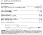
current rating.png

This is the current rating given in datasheet.200mA is maximum current current all ports...20mA by I/O pins.
It having 8 relays also.So the total consumable will come nearly to the maximum value given by the manufacturer.

How to avoid this one..?

Is their any other driver to use for more efficiency.
 

As said before, by using suitable drivers for the high current loads. Can be anything like ULN integrated darlington, discrete BJT or MOSFET. Efficiency can be required in different regards, e.g. low voltage drop, small form factor, cost efficient. It's up to you to set the priorities.
 

Status
Not open for further replies.

Similar threads

Part and Inventory Search

Welcome to EDABoard.com

Sponsor

Back
Top