Continue to Site

Welcome to EDAboard.com

Welcome to our site! EDAboard.com is an international Electronics Discussion Forum focused on EDA software, circuits, schematics, books, theory, papers, asic, pld, 8051, DSP, Network, RF, Analog Design, PCB, Service Manuals... and a whole lot more! To participate you need to register. Registration is free. Click here to register now.

DRC Error: N+SD Iso Psub tap spacing must be <=10.0 um

Status
Not open for further replies.

sp.bhuvana

Newbie level 5
Newbie level 5
Joined
Feb 20, 2019
Messages
8
Helped
0
Reputation
0
Reaction score
0
Trophy points
1
Visit site
Activity points
64
Hi, Iam new to Virtuoso Layout L. I tried to simulate LNA using nmoscap from gpdk180. Iam getting an DRC error stating that "N+SD Iso Psub tap spacing must be <=10.0 um". Kindly help me to clear that error
 

Sounds like you need to add a psub tap next to your N+SD.


I have already attached Psub tap to N+SD... Still same error exists... And also tried by attaching IsoPwell tap... still getting same error... Kindly help me...
 

I have already attached Psub tap to N+SD... Still same error exists...

Did you connect the Psub via a contact to M1 to GND? If not, it doesn't work. If yes, you better provide an image of the field of your problem.
 

If the cap is any useful size you probably need more
than "a" Ptap. Why can you not see by the displayed
error marker, where the device check is unhappy?
 

Did you connect the Psub via a contact to M1 to GND? If not, it doesn't work. If yes, you better provide an image of the field of your problem.

Hi Erikl,
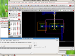
Sorry for the delayed reply. Herewith i have attached the image of my problem. nmoscap_err.png
 

Not sure if I interpret your colors correctly. At the left side to me it seems you have an Nimplant within a Pimplant crossing the Nwell border (connected to the D? of the nmos, pls. see the picture below), which isn't a valid Ptap.
nmoscap_DRC-error.png
At the right side it seems there is one more Pimplant partly within the Nwell (connected to the S?), which isn't a valid Ptap as well.

Valid Ptaps should have a P+diff on psub outside - but not too far (<=10µm , in your case) from - the Nwell border, and then be connected through a contact to ME1 and to GND - not to the Source, and generally also not to the Drain of the Nmos.
 

Not sure if I interpret your colors correctly. At the left side to me it seems you have an Nimplant within a Pimplant crossing the Nwell border (connected to the D? of the nmos, pls. see the picture below), which isn't a valid Ptap.
At the right side it seems there is one more Pimplant partly within the Nwell (connected to the S?), which isn't a valid Ptap as well.

Valid Ptaps should have a P+diff on psub outside - but not too far (<=10µm , in your case) from - the Nwell border, and then be connected through a contact to ME1 and to GND - not to the Source, and generally also not to the Drain of the Nmos.

Hi Erikl,
Actually to the left of NMOS is Nwell Tap(Nwell with Nimp). If i do not connect the Nwell tap, iam getting the DRC error stating that "NBuried Stamp_error Float" as shown in the picture.
And Also as u said, i have connected Psub tap nearer to Nwell, still same error exists... What should i do?
 

Attachments

  • nmoscap_DRC_err.png
    nmoscap_DRC_err.png
    95.2 KB · Views: 417

Status
Not open for further replies.

Part and Inventory Search

Welcome to EDABoard.com

Sponsor

Back
Top