Continue to Site

Welcome to EDAboard.com

Welcome to our site! EDAboard.com is an international Electronics Discussion Forum focused on EDA software, circuits, schematics, books, theory, papers, asic, pld, 8051, DSP, Network, RF, Analog Design, PCB, Service Manuals... and a whole lot more! To participate you need to register. Registration is free. Click here to register now.

DIY USB sharing switch

Status
Not open for further replies.

4kruby

Newbie
Newbie level 4
Joined
Nov 2, 2020
Messages
5
Helped
0
Reputation
0
Reaction score
0
Trophy points
1
Activity points
61
Hello,

I have few designs for a usb sharing switch for keyboard and mouse between my PC and the Raspberry Pi4.
I have searched the internet and many circuits are speculative. So, I wanted some opinions from circuit design experts.

I have no idea about USB. But have a fair knowledge on electronics. Just I do not want to damage the USB ports of the PC or Pi.

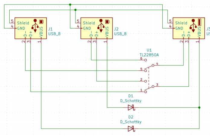
1.
1604331069508.png


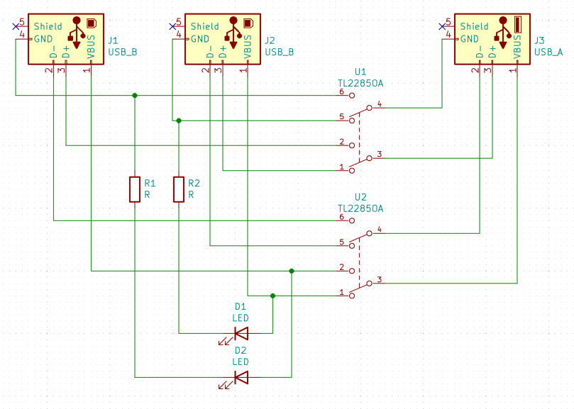
2.
1604331092567.png


3.
1604331111004.png


Can anyone suggest which one would be best? I know option 3 is fool proof. But it requires that every time I am going to push two switches! And I guess option 1 will work as long as the power is drawn from one source.

for Switch, i am considering a push-lock switch like this : https://octopart.com/tl2285oa-e-switch-1166073

I did post this in Raspberry Pi forum but did not get any reply.

My main aim is to share keyboard and mouse AND not to damage the USB port of PC and Pi (I consider eliminating the hub also).

Thank you!
 

The problem I think you will see is that most USB hosts detect that something has been plugged in by looking for it drawing current. That means you have to break the VBUS connection. You might then face a different problem, each time a device is detected it will start the USB enumerator to allocate it a port number, that means switching away and then back to the same USB device might give it a different number. You would have to try it to see what happens as the consequences are really up to the operating system to decide.

Incidentally, those switches are only rated to 100mA, far less than a USB port is capable of supplying. With just a keyboard or mouse you can probably get away with it but even some USB memory devices will overload them. Be careful what you plug in!

Brian.
 

This doesn't answer your question, but...
My wireless mouse came with a little USB dongle. The dongle is a radio receiver, instant plug-and-play. No additional drivers are needed.
wireless mouse w USB connec.png

All you need is a duplicate dongle, then one mouse can control two devices. No switching, no hazard to your valuable devices. (Although I don't know whether all dongles receive on an identical frequency.)

I bought it cheap for ten dollars (I think). I can control my laptop via either the mouse or its built-in trackpad, simultaneously.
 

Thanks Brian,

I will plug only keyboard and mouse.
As you told, this switch is rated for 100mA, I can go for this switch :

But I cannot mount it on a PCB. I mean I can make it mount since I am doing my own PCB. But I have to drill a way bigger hole.

Which circuit would you recommend?

@BradtheRad That costs much where I live and I can go for a KVM switch for that price. So, I am resorting to making my own.

Thanks.
 

That switch is still only going to change over two of the lines, you probably need three to switch VBUS as well and the switches would have to operate simultaneously.

Have you considered using electronic switching? I haven't tried it myself but I would imagine a low resistance analog switch would be able to manage the data signals as long as you were careful with the wiring layout. You could then use the power switch to enable the appropriate signal paths as well.

Brian.
 
Hi Brian,
Now, I have another requirement which I learn from you reply - to switch all the three signals simultaneously - I did not consider this in the beginning (that stems from the ignorance of the USB protocol).
So, if it has to be switched simultaneoulsy I don't have anyother option other than a muliplexer IC.
Can I use this IC? CD4053 ? It can switch three signals. I am not sure whether it can handle USB signal frequency. It also has on-off-on switching pattern.
Also, I don't want to use separate powersupply (from the datasheet I see the current requirements are pretty low for this IC).
Can you please share your thoughts on this?

Thanks.
--- Updated ---

Hi Brian,
Now, I have another requirement which I learn from you reply - to switch all the three signals simultaneously - I did not consider this in the beginning (that stems from the ignorance of the USB protocol).
So, if it has to be switched simultaneoulsy I don't have anyother option other than a muliplexer IC.
Can I use this IC? CD4053 ? It can switch three signals. I am not sure whether it can handle USB signal frequency. It also has on-off-on switching pattern.
Also, I don't want to use separate powersupply (from the datasheet I see the current requirements are pretty low for this IC).
Can you please share your thoughts on this?

Thanks.
I am not able to edit the post. So I am posting the update as reply:

How about the second configuration circuit which uses schottkey to connect the two V+ lines? Is it advisable? But this method, with the available components with me, i can do a "simultaneous switch"

Thanks.
 
Last edited:

You can try this but I can't guarantee it will work:

Use a CD4053 to switch the D+ and D- signals and permanently power it from the source USB VBUS line. Use a single pole change-over switch to change the VBUS power to the mouse OR the keyboard and from one of those, also connect to the address lines of the CD4053.

The idea being that when the power is switched from one to the other it also changes the signal paths of D+ and D- through the CD4053.

Your electrical problem will be the 'on' resistance through the CD4053 is relatively high, it might be better to use a CD4052 with two switches for each path in parallel. There are better two channel analog switches than those you could try. I think you might still have a problem the the enumerator software but you will have to try it out for yourself. Run 'lsusb' in a terminal window and try switching sources. You will have to run 'lsusb' each time, if it shows a new USB device is added to the list after switching you will have a problem, if it shows the same list each time you should be OK.

A mouse and Keyboard are almost certainly low speed USB devices but even so, be careful with the wiring layout. The physical lengths of the data lines should be as close as possible to each other.

Brian.
 
  • Like
Reactions: 4kruby

    4kruby

    Points: 2
    Helpful Answer Positive Rating
Thanks Brian. Let me try some circuits. I am just in designing phase now.
 

Hi I Tried the CD4052 route. Schottky diode to join VBUS works.

scr.png


This CKT is working excellent for low speed devices (1.5Mbps) . FS devices (12Mbps Datarate), is unable to cope up with....

or could it be my badly designed PCB?

sr2.png


I also tried FSUSB73UMX. I am unable to get it working. :(


Anyone with FSUSB73UMX experience?
 

Hi,

The PCB layout is far from being optimal.
especially the GND pin connection of the ouput USB port vias the shielding/case is a no-go.

But there are other issues likely to cause problems:

*don´t leave the A and B pins of the 4052 floating. Use pull up or pull down. and add a third pad for GND. Any A/B wiring needs a suitable reference (GND).

* use a bulk capacitor for 5V and add a 100n ceramics capacitor close to the supply pins of the xx4052

* I wonder how much ON resistance is allowed to be within USB specification. For sure a 74VHC4052 has much lower ON resistance.

* sooner or later I expect that ESD will kill the xx4052. I recommend to install typical USB signal line protection diodes.

Don´t get me wrong... for your own usage it willl not the big problem if it fails. But if you want to sell thousands of them ... I´d improve them ;-)

Klaus
 
  • Like
Reactions: elechi

    elechi

    Points: 2
    Helpful Answer Positive Rating
Adding to Klaus' excellent advice, FS USB is critical of trace lengths, if possible try to match the lengths of D+/D- for each channel. The channels don't have to be the same but the data lines within each channel should be. Your PCB package may have a feature to do this.

Brian.
 
  • Like
Reactions: elechi

    elechi

    Points: 2
    Helpful Answer Positive Rating
Adding to Klaus' excellent advice, FS USB is critical of trace lengths, if possible try to match the lengths of D+/D- for each channel. The channels don't have to be the same but the data lines within each channel should be. Your PCB package may have a feature to do this.

Brian.

Definitely, I agree that matching trace indeed is an issue, as I thought so. But what I read in the CD4052 (Note the CDxxx) that the max frequency response at - 3db was 13MHz could this also be a reason? Should I try with HC Series?
 

Hi,

The PCB layout is far from being optimal.
especially the GND pin connection of the ouput USB port vias the shielding/case is a no-go.

But there are other issues likely to cause problems:

*don´t leave the A and B pins of the 4052 floating. Use pull up or pull down. and add a third pad for GND. Any A/B wiring needs a suitable reference (GND).

* use a bulk capacitor for 5V and add a 100n ceramics capacitor close to the supply pins of the xx4052

* I wonder how much ON resistance is allowed to be within USB specification. For sure a 74VHC4052 has much lower ON resistance.

* sooner or later I expect that ESD will kill the xx4052. I recommend to install typical USB signal line protection diodes.

Don´t get me wrong... for your own usage it willl not the big problem if it fails. But if you want to sell thousands of them ... I´d improve them ;-)

Klaus

Will floating A/B inputs add any cap loading? I thought they were the other end of the turned off TGs and keeping them floating should be okay.

Also, I did not understand the point on adding the third gnd pad and reference for A/B inputs? Could you explain it a bit more?

Datasheet of CD4052 says Ron as 120 ohms. Seems bit higher for USB spec of 90ohms.
 

CD4052 is a very old device and not as good as more modern switches.

Just a thought and I have not tried this:

There are some very inexpensive 'logic level shifter' boards on the market. These typically have four channels each with a signal connection at each side, a 5V supply and a 3.3V supply pin. They are normally used as bi-directional interfaces between 5V logic systems and 3.3V logic systems. On the boards are four FETs (usually BSS123) and some resistors.

If you use two of the boards and ignore two channels on each, I'm pretty sure you can join the high voltage sides in parallel to go to your USB-A and use the low voltage sides to go to the two USB-B connectors. You should be able to switch the boards on or off by grounding (off) or applying 5V (to the 3.3V input). They should work at high speed. If you search you will find the schematic for them, you could build it from discrete components yourself as it is only 3 components per signal route. BSS123 FETs are very inexpensive and easy to buy.

Brian.
 

Will floating A/B inputs add any cap loading? I thought they were the other end of the turned off TGs and keeping them floating should be okay.

Also, I did not understand the point on adding the third gnd pad and reference for A/B inputs? Could you explain it a bit more?
See your own schematic. A and B are the inputs to select which USB channel to use.
They must not float.
You need to control them somehow. It's not shown how you do this. You need to provide this information for further discussion about A and B.
To control them you need at least one power signal, I recommend GND.

Klaus


Oh you refer to that? :) I got it confused with X/Y

The connector on A/B is an off board connector, where I solder jumper wires, which I connect to my bluepill (STM32F103X uC). They aren't floating, and the bluepill also shares the same gnd line. This is a quick (and dirty) design I made to check proof of concept.
 

CD4052 is a very old device and not as good as more modern switches.

Just a thought and I have not tried this:

There are some very inexpensive 'logic level shifter' boards on the market. These typically have four channels each with a signal connection at each side, a 5V supply and a 3.3V supply pin. They are normally used as bi-directional interfaces between 5V logic systems and 3.3V logic systems. On the boards are four FETs (usually BSS123) and some resistors.

If you use two of the boards and ignore two channels on each, I'm pretty sure you can join the high voltage sides in parallel to go to your USB-A and use the low voltage sides to go to the two USB-B connectors. You should be able to switch the boards on or off by grounding (off) or applying 5V (to the 3.3V input). They should work at high speed. If you search you will find the schematic for them, you could build it from discrete components yourself as it is only 3 components per signal route. BSS123 FETs are very inexpensive and easy to buy.

Brian.

The logic level shifter boards available in market are not bidirectional. The usb D+/D- needs full bidirectional (analog) connectivity between host and device.

I also tried the FET method. (BSS84 + 2N7002) And make my own discrete TranGate but the discrete FETS what we get in the market are all 3 terminal devices and have a parasitic diode within.

Screenshot_20201108-104819_Adobe Acrobat.jpg


So it has a full conductivity in one direction (Source to drain) even without device gate turned on.
I tried connecting two devices in series in opposite direction to nullify the effect of the diode. However the TG was much slower compared to CD4052 😕

So I dropped the idea of FET approach.
 
Last edited:

Oh you refer to that? :) I got it confused with X/Y
:) that's why we have schematics with naming the signals/parts ;-)

The connector on A/B is an off board connector, where I solder jumper wires, which I connect to my bluepill (STM32F103X uC). They aren't floating, and the bluepill also shares the same gnd line. This is a quick (and dirty) design I made to check proof of concept.
This exactly is what I thought.
You should wire the according ground along with the A/B wires.
The GND is a part of the A/B signals.
Don't rely on the USB cables as GND. They may carry currents, HF noise ... and increase the ESD problematic.

Now that I hear you use a microcontroller my - more exact - recommendation:
* install pull ups on the 4052 board
* Use GND / OPEN on the microcontroller board to control the A/B lines. The same way as you do with mechanical switches.
This has one "life saving" benefit: in case the USBs are powered down, then the 4052 has no power supply. In this case when you "push" HIGH voltage from the microcontroller to the 4052 you violate it's "signal input voltage range". The inside protection diodes become activated ... current will flow...for longer than just microseconds.

Don't think in hours ... even seconds may be too much time.

If you don't want to use it with this project maybe it's worth to think about with your next project.
General ESD recommendation: put protection on every signal that enters/leaves the PCB.

Klaus
 
:) that's why we have schematics with naming the signals/parts ;-)


This exactly is what I thought.
You should wire the according ground along with the A/B wires.
The GND is a part of the A/B signals.
Don't rely on the USB cables as GND. They may carry currents, HF noise ... and increase the ESD problematic.

Now that I hear you use a microcontroller my - more exact - recommendation:
* install pull ups on the 4052 board
* Use GND / OPEN on the microcontroller board to control the A/B lines. The same way as you do with mechanical switches.
This has one "life saving" benefit: in case the USBs are powered down, then the 4052 has no power supply. In this case when you "push" HIGH voltage from the microcontroller to the 4052 you violate it's "signal input voltage range". The inside protection diodes become activated ... current will flow...for longer than just microseconds.

Don't think in hours ... even seconds may be too much time.

If you don't want to use it with this project maybe it's worth to think about with your next project.
General ESD recommendation: put protection on every signal that enters/leaves the PCB.

Klaus

You are suggesting of an open drain control like the failsafe (power isolation) circuitry of I2C? Definitely for a full blown product it might be a good point to consider. Unless the Vcc of 4052 is connected anywhere but floating, (i do understand the esd diodes get fwd biased) where would the pumped in current go?
 

Update,
With 74HC4052, FS devices are also working perfectly. So this design is good for both FS and LS devices.
Tested with the PCB as in previous post, so definitely, CD* version is slower compared to HC/HCT version.

Additional to this, I added some optocouplers and fully isolated the supply, now supply to 4052 is only from any of the supplies as well as the A/B will be driven from the same supply. Thanks to KlausST for your suggestion.

kvm.png


I will be fabricating a homebrew PCB. I am also trying to take care of the D+/D- path length skew as much possible as suggested by betwixt

I will post the PCB layout once I am done with the board design.

- elechi
 

Status
Not open for further replies.

Part and Inventory Search

Welcome to EDABoard.com

Sponsor

Back
Top