Continue to Site

Welcome to EDAboard.com

Welcome to our site! EDAboard.com is an international Electronics Discussion Forum focused on EDA software, circuits, schematics, books, theory, papers, asic, pld, 8051, DSP, Network, RF, Analog Design, PCB, Service Manuals... and a whole lot more! To participate you need to register. Registration is free. Click here to register now.

Disatrous problem intrinsic to DC restored transformer gate drives.

Status
Not open for further replies.
T

treez

Guest
Newbie level 1
Disastrous problem intrinsic to DC restored transformer gate drives.

Hello,
The attached shows a disastrous problem with a DC restored transformer FET gate drive. (shown here with a cascaded buck SMPS)
…when the converter is suddenly no-loaded from full load, the duty cycle obviously goes fairly quickly to zero. Ater the duty cycle has finally gone to zero, the FET gate voltage of the high side FET lingers high for many switching periods…….BOOM!

As far as we can see, this can only be stopped by very heavy resistive damping…damping which is far too heavy for a transformer gate drive. So what’s the answer?

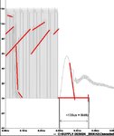
The attached shows the overall schematic, also a Ltspice simulation which demonstrates the problem, and the high side gate drive waveform which shows the FET gate-source voltage lingering high for far too long after D has gone to zero.
 

Attachments

  • Cascaded buck_sudden no load_schematic.pdf
    32.9 KB · Views: 298
  • Txfmr gate drive problem_Vgs waveform.pdf
    113.7 KB · Views: 264
  • Cascaded buck_sudden no load.txt
    18.2 KB · Views: 154

Is this really true? Because PWM duty ought to follow
Vout/Vin unless your powet train is really incapable
of sourcing the load current. And that would show a
really poor full load efficiency.

I can tell you in my integrated POLs, 85-90% FL eff%,
I never saw duty cycle deflect more than a few percent.
But I did have a very nice tight control loop there, and
it's possible that a slow loop with bad error amp overshoot
might act badly.

Can't see on the schematic, the node numbers to tell what
the waveform plot is showing.

Anyway, it's not "obvious" to me why duty cycle should
peg low or high on load dump or apply, unless the error
amp is allowed to "wind up" badly.

If the waveform is really FET Vgs, I'd look back further
in the chain to see why the transformer is not being
switched. Maybe the controller is not appropriate,
maybe you want one that enforces a min and max
duty cycle (not allowing min duty to flicker between
no pulses at all, and runt pulses, and some minimal
well formed on time).
 
  • Like
Reactions: treez

    T

    Points: 2
    Helpful Answer Positive Rating
I dunno....
The whole thing just terrifies me.

I would drive the pulse transformer with a constant 50% 50% duty cycle and just use that to generate isolated gate drive power.
Or else use a commercial dc/dc one watt isolated power module.

Then I would use a proper opto isolated gate driver such as a 3120 to drive the gate.
Guaranteed 0% to 100% drive, total positive on and off lasting forever.

Transient effects and fault conditions can be very unforgiving.

Take a long draught of whisky, bite the bullet, front your boss, and totally redesign whole the evil thing !
 
  • Like
Reactions: treez

    T

    Points: 2
    Helpful Answer Positive Rating
Can't see on the schematic, the node numbers to tell what
the waveform plot is showing.
The waveform shows Vgs of the fet.


it's possible that a slow loop with bad error amp overshoot
might act badly.
The problem is the top post is an intrinsic problem of this type of dc restored transformer gate drive...and there is no way to get rod of this problem without ridiculously large amounts of damping resistance......unless someone has an as yet unknown fix?....I don't think it depends on the speed of the feedback loop, other than it being possibly worse with slow feedback loops.
 

I don't think it depends on the speed of the feedback loop, other than it being possibly worse with slow feedback loops.
The problem won't occur with slower duty cycle variation. If you have both, large duty cycle range, e.g. 0 to about 90 % in your example, and fast d.c. variation, the simple DC restoring circuit can't work.

Like Warspeed, I'm not so motivated to fix this circuit. But it seems to me that the L/R to RC time constant ratio can be better adjusted to avoid slow gate voltage rise to midscale.
 

Even if some kind of compromise "tuning" can improve it, I would still worry about what may happen during initial cold power up, and final power down.
 

Seems like you need a duty cycle range of about 25% min
(400V-100V no load) to maybe 90% max (120V in, 100V
out, full load). Maybe the problem is with the simple cheap
controller. If you had one that let you get ahold of error
amp output, before the PWM, maybe you could clamp the
upper and lower excursions such that chopping never
ceases (which I take to be the root of the problem).

But the idea of creating a flying high side control rail
pair via one pulse xfmr, and controlling some flying
driver with a second xfmr, does seem appealing.
 
  • Like
Reactions: treez

    T

    Points: 2
    Helpful Answer Positive Rating
I would still vote for an opto isolator type gate driver, especially one that has an effective inbuilt under voltage lock out.
 
  • Like
Reactions: treez

    T

    Points: 2
    Helpful Answer Positive Rating
It is MWD application, and we cant use optos due to 170degc ambient
 

It is MWD application, and we cant use optos due to 170degc ambient
Yes, reminds me to the fact that you get paid for designing suitable circuits to deal with this conditions, not we.
 

I would guess your magnetic properties are terrible at high temp but perhaps not included in simulation.

Is the source of the simulation failure not obvious?
 
  • Like
Reactions: treez

    T

    Points: 2
    Helpful Answer Positive Rating
It is MWD application, and we cant use optos due to 170degc ambient

Similar to other complaints, which seem to come from a
literal reading and belief in the comprehensive truth of
datasheets. But what makes an optoisolator unusable
at "high" temp? 170C is not particularly high, a BJT is
going to leak some and saturate worse but not just die
abruptly at 125.1C; LED neither. Maybe your barrier
glop decomposes but I'd doubt that too. Have you shown
that there is not one opto that can, with proper design,
do the job? Or are you just letting paper hold you back?
 

Yes, the DC restoration circuit has problems with fast changes in duty cycle. This is a well known issue which I've always seen described in app notes, and has to be considered with the controller design. If you need fast transient response, then don't use the circuit.

Similar to other complaints, which seem to come from a
literal reading and belief in the comprehensive truth of
datasheets. But what makes an optoisolator unusable
at "high" temp? 170C is not particularly high, a BJT is
going to leak some and saturate worse but not just die
abruptly at 125.1C; LED neither. Maybe your barrier
glop decomposes but I'd doubt that too. Have you shown
that there is not one opto that can, with proper design,
do the job? Or are you just letting paper hold you back?
You're not wrong, but who has the time and resources to spend vetting a component beyond its specifications for a single contract? That's why designs like this are best left to companies who deal with these design challenges specifically. They must have a list of components whose operation at high temperature has been studied rigorously; information they keep for themselves.
 

Thanks Mtwieg, you are of course right to say that it is sudden change of duty cycle that causes this, however, it surprisingly doesn’t relate to the feedback loop speed of the smps…..as you can see, the smps in the top post has a quite slow feedback loop, but the gate drive waveform, despite initially slowly changing in duty cycle, then suddenly goes to zero……this is unavoidable when this control chip is used….and of course, it results in the shown problem occurring. We cannot change the control chip because we don't know if an alternative would be ok at the high temperatures

- - - Updated - - -

Is the source of the simulation failure not obvious?
Thanks, yes it is now obvious, but there seems to be no alternative.
 

Yes, the DC restoration circuit has problems with fast changes in duty cycle. This is a well known issue which I've always seen described in app notes
thanks but please tell where, because I have never seen this described anywhere, ever.

To think, in 2015, the SMPS fraternity does not have an answer for a reliable high side gate transformer fet drive that can do 0 to 95% duty cycle, and go to zero duty cycle without this potentially massively destructive problem. Of course, as DickFreeBird said, two pulse transformers can be used...one to give the power, one to pass the gate drive as a signal.

- - - Updated - - -

Yes, reminds me to the fact that you get paid for designing suitable circuits to deal with this conditions, not we.
Get payed? Is there money in Fracking? I don't think so.
 

Process controls for parts designed to operate at extreme temperatures beyond Mil-Spec range of 125'C are quite different and also tend to use glass passivation in ceramic as I suggested with LTI parts.

I did not find a single Optoisolator rated beyond 125'C.
This one is quite interesting 0.5 Amp Output Current IGBT Gate Drive Hermetic Optocoupler
The Mil-Spec price was quite interesting too.
https://www.digikey.hk/product-detail/en/HCPL-5151-300/HCPL-5151-300-ND/2211350


I know that the epoxy used for clear LEDs has a much lower glass transition temp but don't know what type of epoxy is used in sealed isolators.

If you do find anything , i guarantee it will be cost prohibitive.

I remember for TV signals we used a pulsed switch to DC restore the ac coupled signal < 1us but those were higher impedances. "Active clamp pulse"
 
Last edited:
  • Like
Reactions: treez

    T

    Points: 2
    Helpful Answer Positive Rating
I tried running the simulation and I think there must be something wrong with the controller's model. There doesn't seem to be any coherent relationship between the error amplifier output and the peak CS voltage.

- - - Updated - - -

thanks but please tell where, because I have never seen this described anywhere, ever.
I know the classic unitrode app notes cover it.

To think, in 2015, the SMPS fraternity does not have an answer for a reliable high side gate transformer fet drive that can do 0 to 95% duty cycle, and go to zero duty cycle without this potentially massively destructive problem.
It's part of the physics of how a transformer works. The standard solution is to use an actual gate driver with an isolated power supply, and use an optoisolator for signal isolation. Even for signal isolation, 0-95% probably isn't feasible for a transformer, unless you use a more sophisticated modulation scheme using narrow trigger pulses (like how is done in some monolithic gate driver ICs).
 
  • Like
Reactions: treez

    T

    Points: 2
    Helpful Answer Positive Rating
The standard solution is to use an actual gate driver with an isolated power supply, and use an optoisolator for signal isolation
Thanks, though as you know, with a buck converter, there is no nice leakage L to slow up the rise of current which charges up the fet CDS.......and thus in a buck in CCM, as soon as the high side fet turns on, the entire input voltage...in this case up to 400v, is available to slam the fet VDS from 0v TO 400v in very quick time....greater than 50v/ns, which violates the transient immunity dv/dt of these kind of signal isolator chips which run the gate drive signal up to the high side fet drive.

- - - Updated - - -

I tried running the simulation and I think there must be something wrong with the controller's model. There doesn't seem to be any coherent relationship between the error amplifier output and the peak CS voltage.
Thanks, but seems a bit unusual (hope its not a windows problem), I just downloaded it from the top post and it works fine for me….the load goes no-load at 3.5ms. By the way I use the “Alternate 2” solver and the “modified trap” thing, (in the hammer icon, under “spice” tab)...ive just been googling to see how to specify "alternate" solver in the ltspice schematic as a spice directive, but cant find out how to do this....thought it would be ".options alternate", but that doesn't work.
 
Last edited by a moderator:

Transformer and coupling caps response needs to be match both spectrum of signal and dynamic impedance.

... perhaps a switched load on gate when you want it off (pulsed gate shunt)


Can you choose a different waveform colour, other than lime green on white?
treez1.jpg
 
  • Like
Reactions: treez

    T

    Points: 2
    Helpful Answer Positive Rating
Have you seen this ap note from IR on wide duty cycle gate transformer drive. It does not have the coupling capacitor in the secondary so this may help with your oscillation problem.
 

Attachments

  • IR-GateDriveWitAuxFetForLargeDutyCycles an-950.pdf
    38.9 KB · Views: 202
  • Like
Reactions: treez

    T

    Points: 2
    Helpful Answer Positive Rating
Status
Not open for further replies.

Similar threads

Part and Inventory Search

Welcome to EDABoard.com

Sponsor

Back
Top