Continue to Site

Welcome to EDAboard.com

Welcome to our site! EDAboard.com is an international Electronics Discussion Forum focused on EDA software, circuits, schematics, books, theory, papers, asic, pld, 8051, DSP, Network, RF, Analog Design, PCB, Service Manuals... and a whole lot more! To participate you need to register. Registration is free. Click here to register now.

Diode clamp and GNDing

Status
Not open for further replies.

boylesg

Advanced Member level 4
Joined
Jul 15, 2012
Messages
1,023
Helped
5
Reputation
10
Reaction score
6
Trophy points
1,318
Location
Epping, Victoria, Australia
Activity points
11,697
If you have a diode clamp (using 1n4148 for example) on the input of logic gate, then would that pin then still be regarded as floating?

Would you still need a large value resistor to GND in order to give it a definite state as far as the logic gate goes?
 

Not sure what you mean by a "diode clamp". Do you mean a diode connected from the input to the positive supply? Ground? If it's a diode connected to the positive supply (with the anode connected to the input, then it's going to look like a floating input. For the cathode connected to ground, you then need to know what the input structure of the logic gate is, i.e., is there enough voltage/current to forward bias the diode?
 

Barry as in preventing voltage spikes above vcc and below gnd. But you have answered my question - I need a high value resistor to gnd to give it a definite state.
 

That's generally good practice.
So on the board that contains my logic chips I put 560k resistor to GND on my aerial inputs where they will plug into the board.

So my ar$e is covered both while I am testing my driver with fixed voltage inputs to those pins and also when I plug in the output from my second board, which contains the actual aerial input passing through schmitt trigger inverters and with the clamping diodes.
 

On another thread you show diode clamps to ground that kill any signal input. Cmos logic ICs already have diodes to clamp input voltages to one diode drop above the supply voltage and to one diode drop below ground but they are tiny with a low max current rating. Also I mentioned that you probably need a series resistor to limit the current from static electricity.
 

On another thread you show diode clamps to ground that kill any signal input. Cmos logic ICs already have diodes to clamp input voltages to one diode drop above the supply voltage and to one diode drop below ground but they are tiny with a low max current rating. Also I mentioned that you probably need a series resistor to limit the current from static electricity.

But remember I am not using CMOS logic chips, rather the HEF/CD ones.

The diode clamp in my case is on the input of an aerial that picks up noise from a tesla coil.

I just wasn't sure whether a diode clamp would give the trace/wire a definite state of GND. I suspected it wouldn't, but I was not sure.

But thinking further, before it reaches my logic gate, the input signal from my aerial passes through two schmitt trigger inverters. So this would give it a definite state before it reaches the input of my logic gate.

But I will keep my two 560k resistors for testing purposes - I doubt they will have any effect on the output of the schmitt triggers.

- - - Updated - - -

On another thread you show diode clamps to ground that kill any signal input. Cmos logic ICs already have diodes to clamp input voltages to one diode drop above the supply voltage and to one diode drop below ground but they are tiny with a low max current rating. Also I mentioned that you probably need a series resistor to limit the current from static electricity.

I am confused AudioGuru.

I thought that CMOS chips were all 5-7V Vcc.

Jaycar have CD4081BC listed on their website:
https://www.jaycar.com.au/medias/ZC4081-dataSheetMain?context=bWFzdGVyfGltYWdlc3w5OTA1OXxhcHBsaWNhdGlvbi9wZGZ8aW1hZ2VzL2hkOC9oZmUvODgzMjIxOTYxMTE2Ni5wZGZ8YTg4NTM2YWJhOTkxZDJmMzk2NTc3NTQ2NWIwMjRkNjZjNTVhMWM0MjBmMzg1NzkyZjQ4MjIwMjk0NGFlNDY5OA

This clearly says that 4081 is CMOS.

But what I actually bought was NXP HEF4081 - presumably it is equivalent to Fairchild CD4081.

But the datasheet for this does not state that it is CMOS,

You are telling me that HEF4081 and CD4081 are just manufacturer names for the same device.

So I don't really know what I have! A CMOS or TTL chip?

- - - Updated - - -

Here audioguru, by looking in the CMOS section of Multim 12 database I found the actual logic chips that I am using in my real circuit.
There being 15V, 10V and 5V versions of CMOS....which I did not know about. And the NXP datasheet I have also mentions 15V, 10V and 5V versions although I did not notice the word CMOS any where in the document.

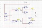
GateDriver_.jpg

So this makes it some what easier to get my TIP base resistors right.
 

Attachments

  • Logic AND HEF4081B.pdf
    127.6 KB · Views: 65

I do not know why Philips (NXP) call their CD4xxx Cmos family "HEF4xxx". Their Family Spec's clearly state that they are CMOS.
On your other thread about this (why so many threads?) I asked why your HEF4081 has an output as high as +15V and a high output current when the datasheet of a CD4081 from Texas Instruments has a graph that shows a typical output voltage loss of 10V! If you calculate the voltage loss with that current then it will be smoking!

I think your simulation software is garbage with many things wrong with it.
 

Attachments

  • NXP HEF4xxx Cmos ICs.png
    NXP HEF4xxx Cmos ICs.png
    13.9 KB · Views: 72

Audio I have little doubt that multisim is garbage when it comes to a commetcial electronic engineer like yourself I presume. But for my simple hobby circuits it is generally good enough. It gets me in the ball park at least and then I can refine things with multimeter and scope.
Is there any better way to buffer the logic chip against the darlingtons than what I came up with?
 
Last edited:

You do not need a Sim program that does things wrong. Instead you just need the datasheets and a little simple arithmetic.
You want 4.47A into 2 ohms which is 8.94V. Then the negative output is +1.53V and the positive output is +10.47V. The circuit cannot do it because the voltage drops are too high.

Let us see if the circuit can make 3A into 2 ohms= 6V. Then the negative output is +3V and the positive output is +9V. It is probably possible.
The base-emitter voltage of the TIP120 with 3A is 2.5V max or maybe 2V typically. The base-emitter voltage of the TIP125 is the same.
The current gain at 3A is typically 1000 so the base current is only 3mA. The CD4081 with a current of 3mA and a supply of 12V has a voltage drop of typically +11.5V so the output of the darlington will typically be +9.5V.
The PNP darlington has the same voltage drops so the output will be +2.5V.
The total output current into 2 ohms will be a little higher than 3A.

The CD4081 will heat with 0.5V x 3mA= 1.5mW which is nothing (its max is 100mW).

If the CD4081 and the darlingtons have minimum specs then the output current will be less.
 

I worded it wrong. The CD4081 with a current of 3mA and a supply of 12V has a voltage output of +11.5V so the output of the darlington will typically be +9.5V.
 

Status
Not open for further replies.

Part and Inventory Search

Welcome to EDABoard.com

Sponsor

Back
Top