Continue to Site

Welcome to EDAboard.com

Welcome to our site! EDAboard.com is an international Electronics Discussion Forum focused on EDA software, circuits, schematics, books, theory, papers, asic, pld, 8051, DSP, Network, RF, Analog Design, PCB, Service Manuals... and a whole lot more! To participate you need to register. Registration is free. Click here to register now.

Differential to single ended amplifier compensation

Status
Not open for further replies.

fpmkh0

Newbie level 6
Newbie level 6
Joined
Apr 18, 2021
Messages
11
Helped
0
Reputation
0
Reaction score
0
Trophy points
1
Activity points
118
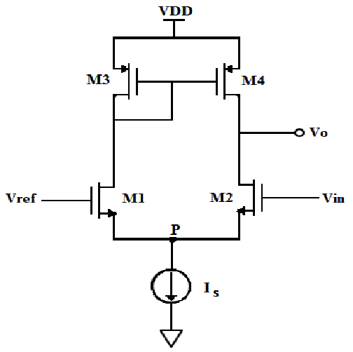
Hi, I want to use differential to single-ended amplifier architecture for the error amplifier in my CMFB loop. I see that in my design, the amplifier does not have a good phase margin. But I haven't seen much information in textbooks about how to compensate for such an amplifier. Razavi warns in his book that such an amplifier might suffer from stability problems due to the mirror pole (compared to a fully differential amplifier), but I could not find in his book talking about compensating for such an amplifier. Can we do something like Miller here? If not, what are the measures I should take to stabilize the amplifier while maintaining its high gain? Thank you.
1682270099804.png
 

1.
Your Vref & Vin need to be at high enough bias voltage so it turns on the transistors. If bias is insufficient then the current source tries to apply negative polarity in order to make current flow... causing your amplifier to be no longer single-ended.

2.
Decide what volt levels you want to appear at nodes. Do you want Vo to read supply V/2 when input is idle? Your mosfets operate like a resistive divider. Configure biasing so that M2 & M4 adopt identical resistance.
Experiment with supply voltage, Vref, etc., so that you obtain desired performance.

3. Experiment with load resistance. My simulations suggest 1k to 10k. With no load I get extreme swings of output voltage.
 

Hi, I want to use differential to single-ended amplifier architecture for the error amplifier in my CMFB loop. I see that in my design, the amplifier does not have a good phase margin. But I haven't seen much information in textbooks about how to compensate for such an amplifier. Razavi warns in his book that such an amplifier might suffer from stability problems due to the mirror pole (compared to a fully differential amplifier), but I could not find in his book talking about compensating for such an amplifier. Can we do something like Miller here? If not, what are the measures I should take to stabilize the amplifier while maintaining its high gain? Thank you.
I do not expect any stability problems with the above shown circuit.
A small and critical phase margin can appear in a circuit with feedback only - where is the feedback loop?
More than that, a phase margin is defined (and can be determined) for the loop gain only. Again: Where is a loop?
 

I do not expect any stability problems with the above shown circuit.
A small and critical phase margin can appear in a circuit with feedback only - where is the feedback loop?
More than that, a phase margin is defined (and can be determined) for the loop gain only. Again: Where is a loop?
As mentioned, this amplifier is used in a CMFB circuit which I haven't shown. Regarding the stability problem of this amplifier, just like other stability simulations, a unity feedback is applied (for the worstcase). So consider input (Vin) directly connected to output (Vo).
 

As mentioned, this amplifier is used in a CMFB circuit which I haven't shown. Regarding the stability problem of this amplifier, just like other stability simulations, a unity feedback is applied (for the worstcase). So consider input (Vin) directly connected to output (Vo).
OK - it seems that I have misunderstood the original question. Sorry for that.
One alternative for improving the phase margin is to use a classical external compensation method (as it is used for uncompensated opamps):
Insert a series combination R-C between the signal input Vin and ground.
So the loop gain for low frequencies (including DC) is not altered, but the loop gain for frequencies in the "critical area" is lowered as much as necessary.
The corresponding time constant RC and the value for R can be found by analyzing the loop gain in the Bode diagram.
 
  • Like
Reactions: fpmkh0

    fpmkh0

    Points: 2
    Helpful Answer Positive Rating
OK - it seems that I have misunderstood the original question. Sorry for that.
One alternative for improving the phase margin is to use a classical external compensation method (as it is used for uncompensated opamps):
Insert a series combination R-C between the signal input Vin and ground.
So the loop gain for low frequencies (including DC) is not altered, but the loop gain for frequencies in the "critical area" is lowered as much as necessary.
The corresponding time constant RC and the value for R can be found by analyzing the loop gain in the Bode diagram.
I see that can help, thank you. Maintaining high UGB while doing this across process is a little bit challenging. But exploiting it not aggressively can help a little.
 

Status
Not open for further replies.

Part and Inventory Search

Welcome to EDABoard.com

Sponsor

Back
Top