Continue to Site

Welcome to EDAboard.com

Welcome to our site! EDAboard.com is an international Electronics Discussion Forum focused on EDA software, circuits, schematics, books, theory, papers, asic, pld, 8051, DSP, Network, RF, Analog Design, PCB, Service Manuals... and a whole lot more! To participate you need to register. Registration is free. Click here to register now.

Differential Amplifier Calculations

Status
Not open for further replies.

strahd_von_zarovich

Advanced Member level 4
Full Member level 1
Joined
Sep 25, 2015
Messages
119
Helped
1
Reputation
2
Reaction score
3
Trophy points
1,298
Activity points
2,475
Hi Everyone,

I am trying to understand what did I do wrong. When I set all the capacitors the same value and impedance of R2||C5 to R1 , the output should be V2-V1 and if they are also equal then the output should be zero. However, in LTSpice, I cant get the same result.
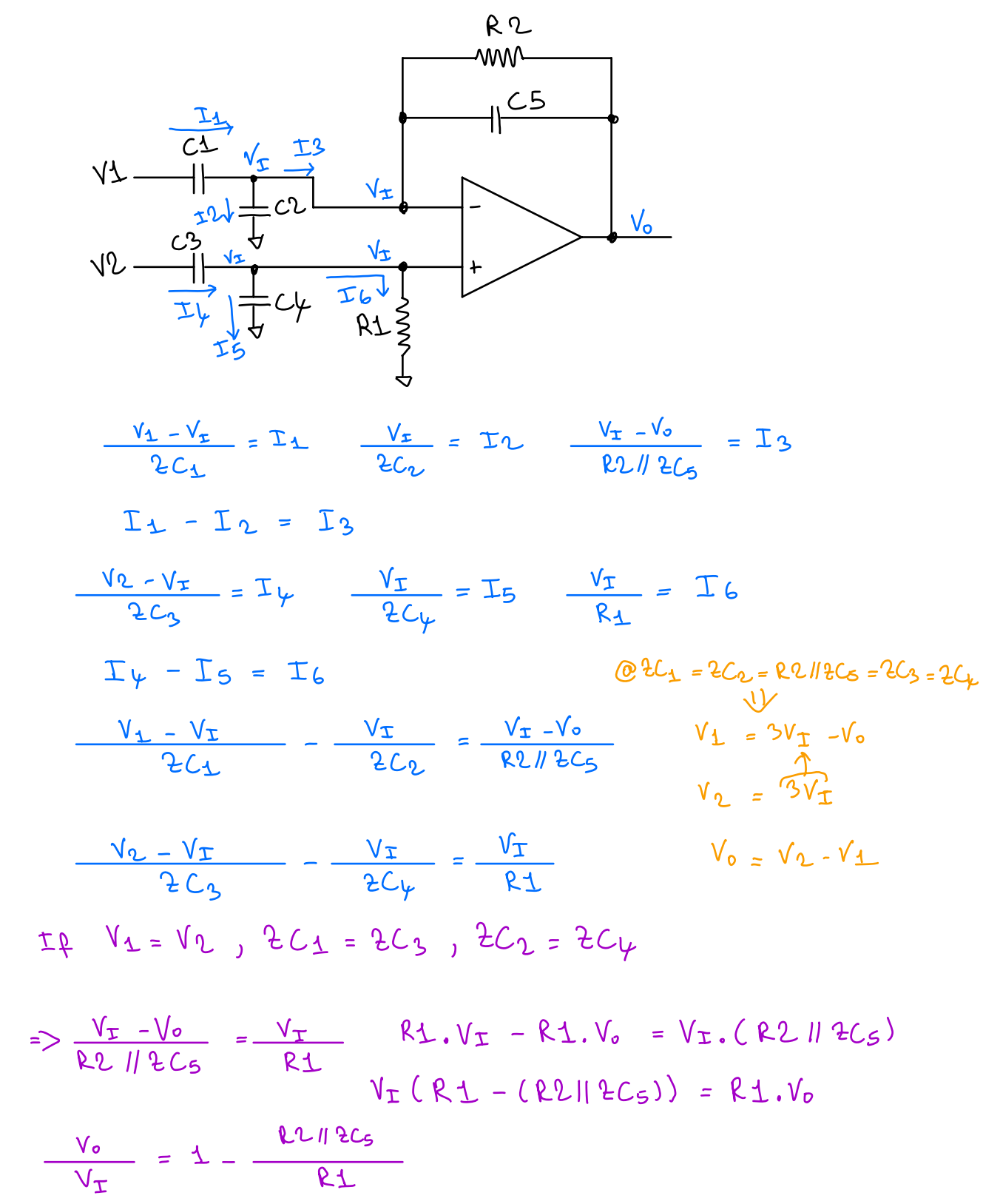
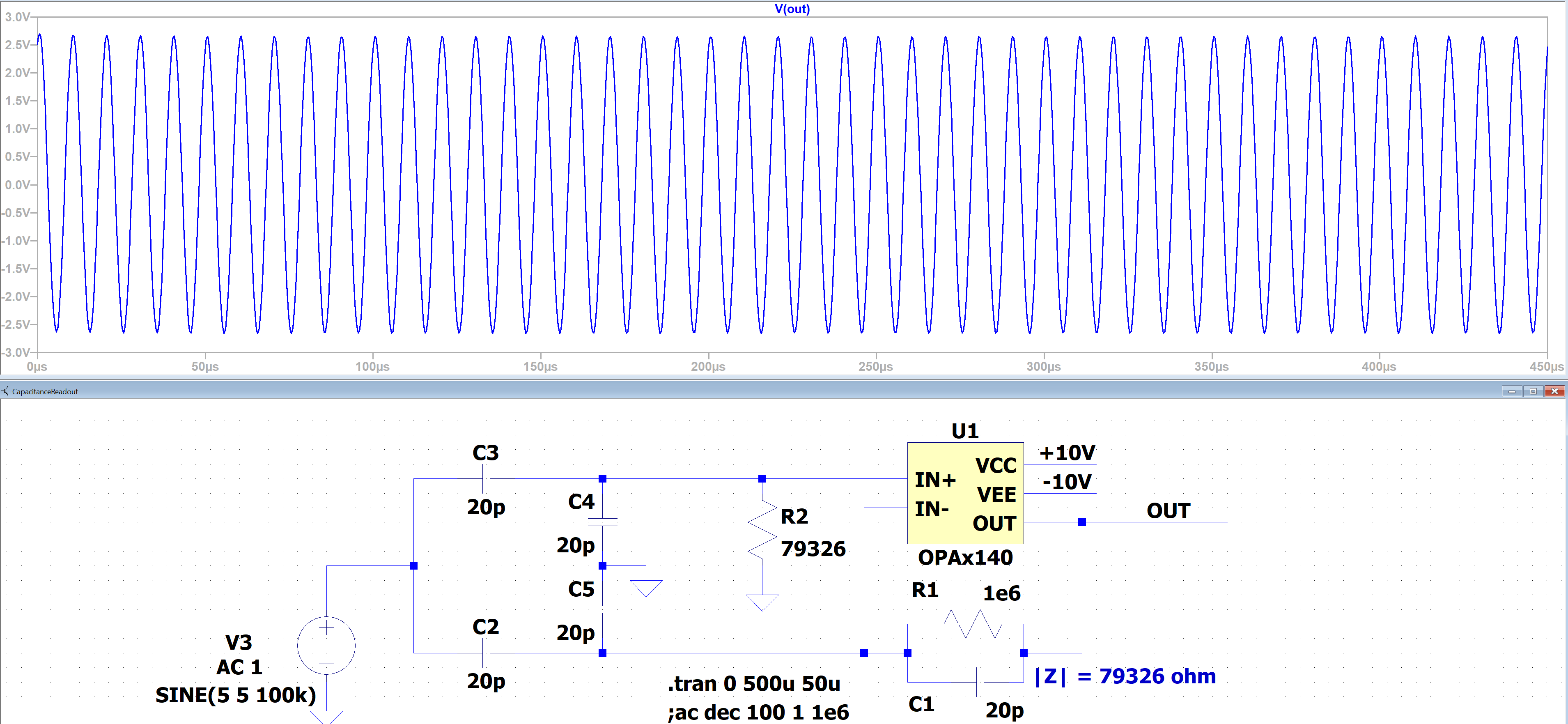
R1.png


R3.PNG
 

Hi,

the shown circuit has different input impedance for V1 and V2.
Thus a signal at V1 generates not necessarily the same output (ignoring the sign) as a signal at V2.
Source imedance also has impact.
If you need equal input impedance (for equal behaviour) you need an instrumentation amplifier topology.

Klaus
 

The input Z appears to be the same as measured at OpAmp inputs :

1691621422598.png


Which makes sense due to - fdbk forcing the inputs to see the 79 K R due to
virtual ground.


Regards, Dana.
 

Hi,

@OP:
Z is not R. Even if you calculate the same value. You ignore the phase shift.
I´m not sure what you want to achieve.
But if you want a true "symmetric difference amplifier" this topology won´t work.
Read documents about
* your single OPAMP difference amplifier circuit, it´s benefits and drawbacks
* true instrumentation amplifier

@dana:
I talked about V1 and V2. Not the very OPAMP inputs.
Do a test:
* put V1 to GND, input 1V RMS sine to V2, measure the current (or the impedance) at V2
now do it the other way round:
* put V2 to GND, input 1V RMS sine to V1, measure the current (or the impedance) at V1

Is the result the same?

Klaus
 

Yes, both V1 and V2 exhibit the same Z. Looks like :

1691627177694.png


When I did it at OpAmp inputs since they are at the same V that produces the same
result as in that case V1 and V2 are at Z = 0 due to driving V source, and the circuit,
bing driven by effectively a V source to set the OpAmp inputs at same V shows same
behaviour, eg. passive (effectively) two port with forward and reverse transmission same......

Regards, Dana.
 
Last edited:

Hi,

This is not the test I was asking for.

And I only see C3, so only one input.

It does not compare the one with the other.

***

below Figure 1 it says:
Although most designers are comfortable with this simple building block, I find that one aspect of their use is commonly overlooked: the two inputs of a difference amplifier have different effective input resistances. By “effective input resistance,” I mean the input resistance resulting from both the internal resistor values and the op amp’s operation.

Klaus
 

Yes, obviously the equivalent of C5 is missing to give zero output with V1=V2. I must confess that I didn't go through the lengthy calculations, but the symmetry condition can be seen without calculation.
 

Hi,

This is not the test I was asking for.

And I only see C3, so only one input.

It does not compare the one with the other.

***

below Figure 1 it says:
Although most designers are comfortable with this simple building block, I find that one aspect of their use is commonly overlooked: the two inputs of a difference amplifier have different effective input resistances. By “effective input resistance,” I mean the input resistance resulting from both the internal resistor values and the op amp’s operation.

Klaus
I grounded one input, drove the other, as you requested. Then switched the driven and grounded
input to do the other side. But just posted one graph as both graphs/results the same.

So then ran it, not using Z probe, but just monitoring current into input caps, and
there is a difference, one sees NI input 80 uA at 1 Mhz, the other INV input 109 uA a
1 Mhz. Note because of input Cap sizes, down <= 10 Khz plots the same all the way
down to DC. Eg. INV nd NI Zin essentially the same. That I believe is because of resolution
of graphs and cursor tools to read out graph values.

So conclusion is INV Zin < NI Zin as Klaus posted. Note this would be affected by
OpAmp used, and its internal comp, but just the values found, not the relationship
that INV Zin < NI Zin


Regards, Dana.
--- Updated ---

Correction, just re-read the 1 Hz values and they are 125 pA NI input, 129 pA INV input.

So inconsistency with TI ap note, but is SPICE model of OpAmp the issue here....?


Regards, Dana
--- Updated ---

Here is Easy Peasy add 20 pF more to C across R1 on the NI path.


1691666076834.png


Regards, Dana.
 
Last edited:

Status
Not open for further replies.

Similar threads

Part and Inventory Search

Welcome to EDABoard.com

Sponsor

Back
Top