Continue to Site

Welcome to EDAboard.com

Welcome to our site! EDAboard.com is an international Electronics Discussion Forum focused on EDA software, circuits, schematics, books, theory, papers, asic, pld, 8051, DSP, Network, RF, Analog Design, PCB, Service Manuals... and a whole lot more! To participate you need to register. Registration is free. Click here to register now.

Different output of Amplifier with slightly changes at input side

Hayee

Member level 3
Member level 3
Joined
Mar 4, 2022
Messages
60
Helped
1
Reputation
2
Reaction score
3
Trophy points
8
Activity points
607
Hi Guys,
I am looking at the following 3 circuits. all of 3 circuits are slightly different but their outputs are different.
Circuit A has a scaled down output (full sinewave) with DC shift.
Circuit B has a scaled down output (half sinewave) with no DC shift
Circuit C is giving pulses at output act as a zero crossing.

I want to know that how to mathematically calculate the resistance values and how these slightly difference in configuration make different output. Mean how I know that by doing this I will get these responses
Kindly guide me


circuit_A.jpg

circuit_B.jpg

circuit_C.jpg


Thanks
 
Hi,

The usual way is:
* FIRST you have a task, a problem ... to solve. It is defined by specifications, by requirements, .. usually numbers with units.
* THEN you look for a suitable circuit .. to fulfill your requirements. OPAMP circuits are well documented, all behaviour is explained, formulae are given.
* THEN you do the math according the law of physics.

BUT you do ... FIRST taking random (for us) circuits and .. you seem to test them.
THEM you try to find (backwards) why they act the way they do.
All circuits act like expected.

You give no information where the circuits are from. These sources usually give the necessary context ... to know how they work, the use cases, the limits ...

****
All circuits seem to be randomly modified (by you?) ... and some miss informations.

1st circuit:
* What voltage is R7 connected to?
* why is R7 value different from R13 value?
* What is the use of R3 and R6?

2nd circuit:
* You can not expect negative output voltage while the supply voltage is not negative. In other words: The output voltage can only be within the supply voltage rails.

3rd circuit:
* You simply overdrive the -INP to a non allowed level. --> keep on datasheet
* missing negative output --> see 2nd circuit

***
Again: My recomendation: Do the learning/designing in the right order. From theory to practice.
In times of internet (we did not have) use it. There are so many good tutorials. All for free, all accessable within seconds.


Klaus
 
Input is AC line, R7, R9 connected to neutral ? And for purposes of sim
circuit ground is at same potential as Neutral ?

The mathematical approach is write node/loop equations and model, for your
purposes, the OpAmp as (where A is quite large, 25,000 min for LM258A, Zin also
quite large, I would ignore, eg. let it be infinity) :


1730284367765.png


After you write the equations you will see that large A (gain) in the opamp many
terms in the equations drop out in the limit, and simple equations are left. Do
a simple case to get a feel, ground + input, place a R output to - input, place a R
from input V source to - input, and solve with that model. Then evaluate the
resulting equation letting A go to infinity. Assume Zin infinity (not even in the circuit),
and Zout 0 for simplicity. More exact analysis takes into account those effects,
especially as A drop with increased frequency, and has large effects on OpAmp
circuit at high frequency as OpAmp gain approaches 0. The AC model for OpAmp looks like
a high DC A (gain) followed by a low pass filter, eg, A rolls off as freq increases.
But dont tackle the AC effects as you seem to be doing AC line freq work where
A is still quite large.

 
Last edited:
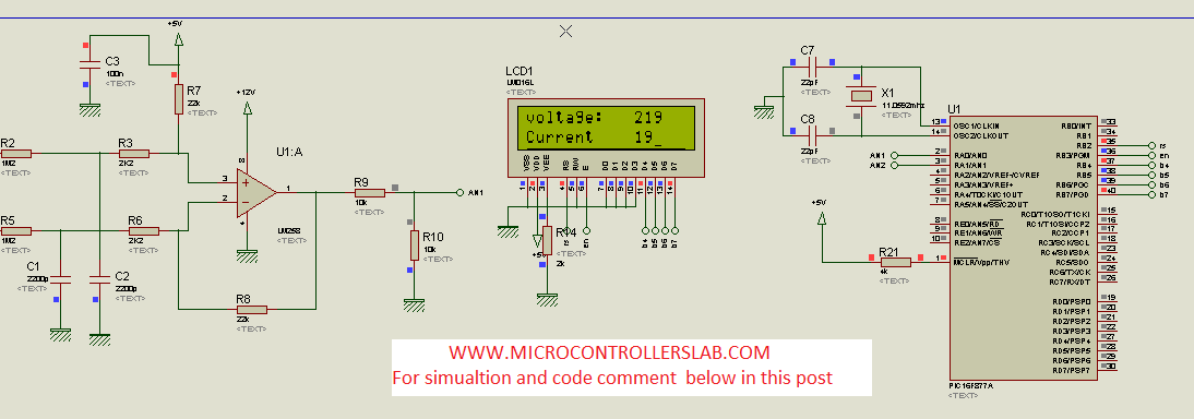
Here is the original circuit

1st circuit:
* What voltage is R7 connected to?
* why is R7 value different from R13 value?
* What is the use of R3 and R6?
R7 and R9 is connected to 5v.
I was seeing this circuit on internet and just tried to simulate this on the software to check the results.
Then i do changes to see the behavior of the circuits.

2nd circuit:
* You can not expect negative output voltage while the supply voltage is not negative. In other words: The output voltage can only be within the supply voltage rails.
will R7 and R9 not add the DC biasing and shift the waveform?

3rd circuit:
* You simply overdrive the -INP to a non allowed level. --> keep on datasheet
* missing negative output --> see 2nd circuit
overdrive the -INP? How you check it and how i can see all these things by myself?
 
overdrive the -INP? How you check it and how i can see all these things by myself?
My bad: it should be "+INP". You overdrive +INP.
And to check a node voltage, simply connect it to your scope. And look at the datasheet what it specifies for +INP.

Everything is well explained in the site you linked to.
I´ve seen only minor mistakes.

So if you want to understand the circuit --> read the text in the link
If you have problems in understanding the text --> ask a detailed question with referencing the text.

Klaus
 

LaTeX Commands Quick-Menu:

Part and Inventory Search

Welcome to EDABoard.com

Sponsor

Back
Top