Continue to Site

Welcome to EDAboard.com

Welcome to our site! EDAboard.com is an international Electronics Discussion Forum focused on EDA software, circuits, schematics, books, theory, papers, asic, pld, 8051, DSP, Network, RF, Analog Design, PCB, Service Manuals... and a whole lot more! To participate you need to register. Registration is free. Click here to register now.

Different between N+ , N- , and N type doping

Status
Not open for further replies.

vasaroopak

Member level 1
Member level 1
Joined
Sep 17, 2010
Messages
41
Helped
8
Reputation
16
Reaction score
8
Trophy points
1,288
Location
Greater Noida, India
Activity points
1,513
Hello All

what is the different between N+ , N- , and N type doping ?
what N+/N- double diffusion ?

Thanks and Regards.
 

Here '+' and '-' indicates the amount charge carriers. In p+ and n+ the number of majority charge carriers will be more.
 
Jushoraj is correct. N + will have more doping of N than N. N - will have less doping of N than N.
 
In simple words we can tell that double diffusion layer permit contact to the substrate from the surface.......................

The Laterally Diffused MOSFET is an asymmetric power MOSFET designed for low on-resistance and high blocking voltage. These features are obtained by creating a diffused p-type channel region in a low-doped n-type drain region. The low doping on the drain side results in a large depletion layer with high blocking voltage. The channel region diffusion can be defined with the same mask as the source region, resulting in a short channel with high current handling capability. The relatively deep p-type diffusion causes a large radius of curvature at the edges, which eliminates the edge effects. Diffusion can be used in addition to further increase the junction depth and radius of curvature.

EDGE EFFECT: Few p-n diodes are truly planar and typically have higher electric fields at the edges. Since the diodes will break down in the regions where the breakdown field is reached first, one has to take into account the radius of curvature of the metallurgical junction at the edges. Most doping processes including diffusion and ion implantation yield a radius of curvature on the order of the junction depth, xj. The p-n diode interface can then be approximated as having a cylindrical shape along a straight edge and a spherical at a corner of a rectangular pattern. Both structures can be solved analytically as a function of the doping density, N, and the radius of curvature, xj.

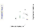
The resulting breakdown voltages and depletion layer widths are plotted below as a function of the doping density of an abrupt one-sided junction.
Figure 4.5.1 : Breakdown voltage and depletion layer width at breakdown versus doping density of an abrupt one-sided p-n diode. Shown are the voltage and width for a planar (top curves), cylindrical (middle curves) and spherical (bottom curves) junction with 1 mm radius of curvature.


https://www.circuitstoday.com/double-diffused-mos-dmos

- - - Updated - - -

The Laterally Diffused MOSFET is an asymmetric power MOSFET designed for low on-resistance and high blocking voltage. These features are obtained by creating a diffused p-type channel region in a low-doped n-type drain region. The low doping on the drain side results in a large depletion layer with high blocking voltage. The channel region diffusion can be defined with the same mask as the source region, resulting in a short channel with high current handling capability. The relatively deep p-type diffusion causes a large radius of curvature at the edges, which eliminates the edge effects. Diffusion can be used in addition to further increase the junction depth and radius of curvature.

EDGE EFFECT: Few p-n diodes are truly planar and typically have higher electric fields at the edges. Since the diodes will break down in the regions where the breakdown field is reached first, one has to take into account the radius of curvature of the metallurgical junction at the edges. Most doping processes including diffusion and ion implantation yield a radius of curvature on the order of the junction depth, xj. The p-n diode interface can then be approximated as having a cylindrical shape along a straight edge and a spherical at a corner of a rectangular pattern. Both structures can be solved analytically as a function of the doping density, N, and the radius of curvature, xj.

The resulting breakdown voltages and depletion layer widths are plotted below as a function of the doping density of an abrupt one-sided junction.
Figure 4.5.1 : Breakdown voltage and depletion layer width at breakdown versus doping density of an abrupt one-sided p-n diode. Shown are the voltage and width for a planar (top curves), cylindrical (middle curves) and spherical (bottom curves) junction with 1 mm radius of curvature.


https://www.circuitstoday.com/double-diffused-mos-dmos
 

Attachments

  • edg.gif
    edg.gif
    7.9 KB · Views: 261
Last edited:

Status
Not open for further replies.

Part and Inventory Search

Welcome to EDABoard.com

Sponsor

Back
Top