Continue to Site

Welcome to EDAboard.com

Welcome to our site! EDAboard.com is an international Electronics Discussion Forum focused on EDA software, circuits, schematics, books, theory, papers, asic, pld, 8051, DSP, Network, RF, Analog Design, PCB, Service Manuals... and a whole lot more! To participate you need to register. Registration is free. Click here to register now.

[SOLVED] designing footprints for QFN packages

Status
Not open for further replies.

abhishekgrover

Newbie level 5
Newbie level 5
Joined
Jul 10, 2015
Messages
8
Helped
1
Reputation
2
Reaction score
1
Trophy points
3
Activity points
93
Hi,
I want to design footprint for QFN48 and QFN16 package.
Please suggest some pdfs or tutorials that I should study to design these footprints in orcad.
Best Regards,
Abhishek Grover.
 

Start with IPC-7351


As to the QFN's the acronym QFN is generic you MUST always specify the pad pitch, body dimension etc. as there are devices with pin pitches 0.5mm 0.65mm 1.0mm etc.
 

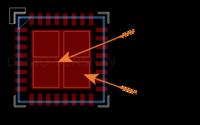
follow the datasheet recommended land pattern or IPC 7351 as reference values for creating the pad. normally 2 types of pads will be there for QFN , (one for normal pads and other for the centre thermal pad) . for Thermal pad you can use exact value given in the datasheet (no extra copper required) . Paste layer can be given as multiple slots for the big thermal pad instead of a single large opening . this can help to avoid the apply of over solder paste
Keep the centre thermal pad as the origin(0,0) of the footprint. Place the other pads to match with your component pitch.
 
A previous reply regarding thermal pads....
A brief summary…
1oz copper is not very good at spreading heat, I have to tweak this area to achieve the more critical requirements in doing so I added some thermal vias as there were none… I could only resume this was because of all the components blocking the way, as the design needed to get the design done I did not want to be back and forth asking questions and as I have done hundreds of designs with these devices on since early 2000 I follow BEST PRACTICE for both reliability and thermal considerations. My go to guide is the IPC specification IPC-7093, but I also have an extensive library covering these components and more specifically PCB thermal design I also refer to a whole bibliotheca of relevant material, a little sample below:
IPC-7093
**broken link removed**

https://www.smtnet.com/library/file...-design-optimal-qfn-yield_reliability-ipc.pdf

https://www.ti.com/lit/an/snva183b/snva183b.pdf

https://www.ti.com/lit/an/snva419c/snva419c.pdf

https://www.cirrus.com/en/pubs/appNote/AN315REV1.pdf

https://www.ti.com/lit/an/snva183b/snva183b.pdf

https://www.vision-systems.com/arti...meras-tackle-pcb-inspection-applications.html

So I can quickly remove the vias, but my recommendation would be to follow industry standard practice with these devices and use thermal vias.
 

Status
Not open for further replies.

Part and Inventory Search

Welcome to EDABoard.com

Sponsor

Back
Top