Continue to Site

Welcome to EDAboard.com

Welcome to our site! EDAboard.com is an international Electronics Discussion Forum focused on EDA software, circuits, schematics, books, theory, papers, asic, pld, 8051, DSP, Network, RF, Analog Design, PCB, Service Manuals... and a whole lot more! To participate you need to register. Registration is free. Click here to register now.

Designing a Class B / Class AB power amplifier

Status
Not open for further replies.

rahdirs

Advanced Member level 1
Joined
May 22, 2013
Messages
424
Helped
93
Reputation
192
Reaction score
91
Trophy points
1,308
Location
Mordor
Activity points
4,492
Hi all,

I need to design a power amplifier that provides a current gain from 25 mA to 10 A keeping the voltage constant.
The input to the power amplifier is an almost constant DC voltage between 11 & 12 V and at 15-25 mA. I need an output at same voltage and 10 A.
There will be no cases of cross-over distortion in my circuit,so i think even class B would work properly

I tried and got only an amplification of 60 as in schematic.
We can't change the impedance of stage next to amplifier
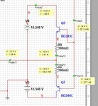
Caure.JPG
 
Last edited:

Are the 390 mOhm resistors supposed to have 10 A going through them? Then they will develop 3.9 V across them. The heat dissipation (wasted) will be 39 watts. This will severely hurt performance.

As you point out, however, it does not reach 10 A. The reason is that the bias voltage must overcome the greater volt level which develops at its emitter terminal, caused by current going through the 390 mOhm resistor.
 

The absolute maximum continuous current allowed for the weak little BD243 and BD244 transistors is only 6A when the base current is very high at 1A.
Connect about 8 transistors in parallel or use power darlington transistors.

The transistors must be biased into class-AB to eliminate crossover distortion. But you have their bases tied together in class-B that produces plenty of horrible crossover distortion.
 

Hi all,

I need to design a power amplifier that provides a current gain from 25 mA to 10 A keeping the voltage constant.
The input to the power amplifier is an almost constant DC voltage between 11 & 12 V and at 15-25 mA. I need an output at same voltage and 10 A.There will be no cases of cross-over distortion in my circuit,so i think even class B would work properly

I tried and got only an amplification of 60 as in schematic.
We can't change the impedance of stage next to amplifier
caure.jpg

Hi rahdirs
The solution is so simple ! use a suitable power transistor like 2n3055 ( or perhaps some 2n3055 in parallel with using some balance resistors ) and then some drivers and then biasing network which can be based on diodes or shunted regulator ! or also a feedback loop ! . that's all you need to do .
Best Wishes
Goldsmith
 

Are the 390 mOhm resistors supposed to have 10 A going through them? Then they will develop 3.9 V across them. The heat dissipation (wasted) will be 39 watts. This will severely hurt performance.
I knew of the 39 W power dissipation in 390mOhm resistance but I read from Sedra and Smith that those resistances used in conjunction with short-circuit protection devices provide thermal stability for the output transistors. Is it OK for me to remove them and save power.

The transistors must be biased into class-AB to eliminate crossover distortion. But you have their bases tied together in class-B that produces plenty of horrible crossover distortion.
In my circuit the input to the power amplifier stays around 13-15 V DC and never goes down to zero & hence cross-over distortion never occurs.

Hi rahdirs
some drivers and then biasing network which can be based on diodes or shunted regulator ! or also a feedback loop ! . that's all you need to do .
Best Wishes
Goldsmith
Can u explain it a bit further on how to use the drivers and the feedback loop u are talking about
 

The absolute maximum continuous current allowed for the weak little BD243 and BD244 transistors is only 6A when the base current is very high at 1A.
Connect about 8 transistors in parallel or use power darlington transistors.

The transistors must be biased into class-AB to eliminate crossover distortion. But you have their bases tied together in class-B that produces plenty of horrible crossover distortion.
As per your suggestion i replaced BD 243 & BD 244 transistors and replaced them with 2N3055 & its complement MJD 2955.The output of my power amplifier was used to charge a non ideal battery of 12 V with internal resistance of 3mOhm. See what happens to current at o/p in schematic in fig.1.It drops down to 1.67uA.

Now i changed a 2N3055 transistor in darlington pair to BD 243 and now i got 40 A current !!!!!!! into the battery and i'm reading -13 V across the battery.Why did my 14 V o/p change to -13 V,shown in fig.2

The circuit was generating 14 V when voltmeter was connected as load & changed to -13 V when battery was attached.
 

Attachments

  • Darlington Power amp.JPG
    Darlington Power amp.JPG
    116.5 KB · Views: 210
  • Darlington 2.JPG
    Darlington 2.JPG
    120.6 KB · Views: 175
  • Circuit.JPG
    Circuit.JPG
    126.2 KB · Views: 160

Why do you have a negative supply and a PNP output transistor that are NEVER used??
Are you making a battery charger? What limits the charging current?

The output transistors should be included in the negative feedback loop of the opamp so there is no voltage drop of two base-emitter junctions.
Then a series current-sensing resistor can be used to limit the charging current and detect when the battery is almost fully charged.


I think your simulation software does not know anything about electronics.
 

Why do you have a negative supply and a PNP output transistor that are NEVER used??
The output transistors should be included in the negative feedback loop of the opamp so there is no voltage drop of two base-emitter junctions.
i have removed the redundant p-n-p transistors which are always off but then the voltage fell down to 1.5 V with current at 22 A as in fig.1.
How do i use them in negative feedback loop??? In fig.2 i have tried using output transistors in negative feedback loop of op-amp but then i get very small currents as 741 can at most supply 30 mA.

Can u provide a blue-print to use power amp in negative feedback to remove that VBE loss i am getting in fig.1.

I will use charge controller circuit after verifying if my circuit is capable of providing 13 V & 10 A to the battery.
Capture.JPGCare.JPG
 
Last edited:

Your opamp driving the darlington pair of transistors is COMPLETELY WRONG and your SIM program knows NOTHING about electronics.

- - - Updated - - -

You had everything connected wrong.

1) The input offset adjustment pins 1 and 5 of an opamp are NEVER connected to ground. Leave them disconnected since you are not adjusting the input offset voltage.
2) The output of the opamp is pin 6 and it MUST drive the base of the BD243 transistor.
3) The negative feedback pin 2 of the opamp should be connected to the emitter of the 2N3055 for negative feedback.

We read from left to right. I turned around your schematic so that the input is on the left side and the output is on the right side.
 

Attachments

  • opamp circuit.png
    opamp circuit.png
    35.7 KB · Views: 171

The absolute maximum continuous current allowed for the weak little BD243 and BD244 transistors is only 6A when the base current is very high at 1A.
How is it that BD 243 in schematic is giving 17 A.
Never,the less why i am still getting high VBE loss.My 741 op-amp is giving an out-put of 16.5 V when max. is 16 V !!!!!

Why is it that you can minimize VBE losses when u you connect it in negative feedback loop of the op-amp???
Why is darlington configuration of BD 243 has lesser VBE losses than other 2N3055 as in schematic ???
Why is darlington config of weak BD 243 is driving higher current than darlington config. of strong 2N3055 ???
 

Attachments

  • BD243.JPG
    BD243.JPG
    99.2 KB · Views: 190
  • mix.JPG
    mix.JPG
    110.4 KB · Views: 147
  • 2N3055.JPG
    2N3055.JPG
    98.7 KB · Views: 163
Last edited:

@Audioguru: What is the use of connecting power amplifier in negative feedback loop of op-amp.I am getting the same values of output voltage & current without using the op-amp. Why is it that the VBE voltage drop that was occuring earlier decreases when transistors were placed in parallel ??

So,why is it that you can decrease VBE loss when connected in negative feedback of op-amp???
 
Last edited:

When the OUTPUT of the transistors are used for the negative feedback to the opamp then the output voltage is THE SAME as the input voltage.
The extremely high open-loop voltage gain of the opamp eliminates the Vbe voltage losses of the transistor (if the supply voltage is high enough).

Again I think your antique SIM software does not work properly.
 
  • Like
Reactions: rahdirs

    rahdirs

    Points: 2
    Helpful Answer Positive Rating
@Audioguru:So,strictly speaking there should be no VBE loss.
Vout of op-amp = A(Vin1-Vin2).
Vin1-Vin2 = Vout/A = approx. zero.
So,the op-amp eliminates the VBE loss.But shouldn't there be a VBE loss of 0.7V if a current flows.

Why is it that VBE loss decreases when output power transistors were connected in parallel??


I am using latest version in Multisim 12.I heard it is quite good.Which one do you use??
 
Last edited:

Pspice, Hspice, Tspice, Spectre , Cadent, Proteus, Caterina , Electronics Workbent , Labview , Synopsis , Symmetic plus, Orcad capture ... etc.:-D
 
Last edited:

Status
Not open for further replies.

Similar threads

Part and Inventory Search

Welcome to EDABoard.com

Sponsor

Back
Top