mustangyhz
Member level 5

power clamp
0.18μm CMOS DIGITAL/ANALOG/RF TECHNOLOGY
TOPOLOGICAL AND RELIABILITY
DESIGN RULES
NOV 2008
Power clamp provides a discharge path between Vdd and ground during ESD event and is
normally off at all other times. Power clamp has been demonstrated in 0.18 um process using
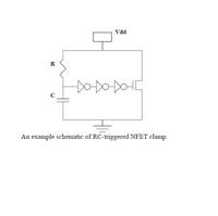
RC-triggered NFET clamp. The clamp has a discharge NFET device, 400/0.4 um, that is
controlled by three inverter stages. The input of the first inverter stage is a RC network (set to
a time constant of ~1.5us). The inverters have been sized to reduce the switching threshold to
reduce the requirement of large R and C. Resistance R is realized by a long channel PMOS.
Capacitance C is realized by NMOS capacitor. This architecture of power clamp is proven in
silicon in 0.18 um technology and it can withstand 1.3A TLP current (equivalent to 2 kV
HBM ESD threshold). Impedance of power clamp at 1.3A is ~3 ohm. Lower impedance can
be realized using wider FETs and smaller silicide block length.

Resistance R is realized by a long channel PMOS.
Capacitance C is realized by NMOS capacitor.
Dose anybody know how to chose the PMOS and nmos?
thanks!!!
0.18μm CMOS DIGITAL/ANALOG/RF TECHNOLOGY
TOPOLOGICAL AND RELIABILITY
DESIGN RULES
NOV 2008
Power clamp provides a discharge path between Vdd and ground during ESD event and is
normally off at all other times. Power clamp has been demonstrated in 0.18 um process using
RC-triggered NFET clamp. The clamp has a discharge NFET device, 400/0.4 um, that is
controlled by three inverter stages. The input of the first inverter stage is a RC network (set to
a time constant of ~1.5us). The inverters have been sized to reduce the switching threshold to
reduce the requirement of large R and C. Resistance R is realized by a long channel PMOS.
Capacitance C is realized by NMOS capacitor. This architecture of power clamp is proven in
silicon in 0.18 um technology and it can withstand 1.3A TLP current (equivalent to 2 kV
HBM ESD threshold). Impedance of power clamp at 1.3A is ~3 ohm. Lower impedance can
be realized using wider FETs and smaller silicide block length.

Resistance R is realized by a long channel PMOS.
Capacitance C is realized by NMOS capacitor.
Dose anybody know how to chose the PMOS and nmos?
thanks!!!

