KlausST
Advanced Member level 7

Hi,
here I´d like to show how to design a DAC controlled high side constant current source
Often used as 0..20mA (or 4..20mA) current loop interface, thus we focus on the interface requirements.
* low speed ( maybe some 10Hz up to some kHz)
* high precision
* low drift
* high stability
* ruggedness
What do we need:
* power source: VCC, GND, Let´s say VCC = 12V
* DAC
* OPAMP
* MOSFET (you could use a PNP transistor, but base current causes an error in load current. Mosfet-gate current is about zero, thus the MOSFET solution is more precise)
* some Rs, Cs, Ds..
I decided to use a "difference Amplifier circuit", because it´s easy to calculate.

* Opamp Supply: every Opamp needs power to operate and it needs a capacitor to stabilize this power supply. 100nF close to the OPAMP is often a good value.
* Difference Amplifier Circuit: simple circuit: R1 = R3, R2 = R4, Gain = R2 / R1
Operation: It simply regualtes the Opamp_output in a way that (V_Feedback - V_OuptutRefernce) = gain x (V_NonInvertingInput - V_InvertingInput)
* DAC: use one with voltage output. This one has an output voltage range 0...5V
* MOSFET: P-Channel, no special one needed. Specifications are: Vcc, I_load, P_tot = VCC x I_Load. Add some headroom to every value.
Current Steering Circuit:
We want to regulate load current.
All load current goes through Mosfet_Drain and Mosfet_Source
..and thus it goes through the shunt (R5).
--> If we know the value of R5 and the voltage across R5 we know the load current.
(1) Thus we feed back (measure) the voltage across R5 to control the load current.
Varying the gate voltage will cause the load current to vary.
To make the P-channnel MOSFET (more) conductive: the voltage at the gate referenced to the source needs to go (more) negative.
(2) The feedback voltage is across R5. This means the feedback voltage is referenced to VCC. Thus we need to connect VCC to the OutputReference of the DifferenceAmplifierCircuit.
(3) The OPAMP_ouptut should control the gate of the MOSFET.
To avoid ringing it´s a good idea to connect OPAMP_output to Mosfet_gate with a resistor. The resistor value is not critical for this low speed application. We use 1kOhms.
(The higher the expected regulation speed the lower the resistor)
(4) The load is connected to Mosfet and GND
Now we need to decide how to connect the DAC:
Imagine: We want: The higher the DACOutputVoltage the higher the load current. And from above we know: The lower the gate voltage the higher the output current.
And because gate voltage = OPAMPOuptut voltage: The HIGHER the DAC voltage the LOWER the OpampOutput voltage. This is inverting operation.
(5) This tells us we need to connect the DACOutput to the InvertingInput
(6) And because the DACOutput is GND referenced we need to connect the NonInvertingInput to GND
Now to the device values:
Shunt: the current is 0..20mA. The voltage drop across the resistor should be large enough to get good measurable feedback voltage, but not too much, because it limits the voltage across the load. Let´s say 2V @ 20mA is a good compromise. --> R = V/I = 100 Ohms
R1, R2, R3, R4: High impedance may cause noise and reduces speed. Low impedance causes high current and thus it stresses the DAC output. For low DAC output current we choose a relatively high value resistor: 100k Ohms. (For sure one could use 10k for lower noise)
This is R1. But we know R3 = R1. Thus R3 is 100k, too.
To get the value for R2 and R4 we need to know the gain: |Gain| = |OutputVoltage / InputVoltage|.
Input voltage is the DAC voltage. 0..5V. Output voltage is the ShuntVoltage = 0..2V.
Thus gain = 2V / 5V = 0.4
Thus R2 = R4 = R1 x 0.4 = 40k (DifferenceAmplifierCircuit formula)
(For a real application I recommend to add some headroom and thus calculate wiith a of 10% higher load current: 22mA --> V_Shunt = 2.2V --> gain = 0.44 --> R2, R4 = 44k)
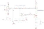
Now the circuit looks like this:

Improvements:
(7) Stability: The path from OPAMP_Output --> R7 --> MOSFET --> R5 --> R2 --> inverting input causes delay. This delay may cause instability, like ringing and continous oscillations.
To avoid this one adds a capacitor directly from OpamOutput to inverting input.
It forms a feedback with cutoff frequency that depends on the parallel circuit of R1||R2. (28k6)
For a 4..20mA loop a cutoff frequency of about 1kHz is a good value. thus C = 1/( 2 x Pi x f x R) = 5.6nF --> use a 4n7nF for C2
(The smaller the capacitor the higher the cutoff frequency, the faster the regulation response, but the higher the risk for instability)
(8) Limiting V_GS:
Especially with higher VCC there is the risk that V_GS of the MOSFET is exceeded by the OpampOutput. Thus a Zener diode is a simple solution to limit V_GS. Zener voltage needs to be less than the V_GS limit.
(9) Limiting V_DS:
Drain signal is the signal to the load. Thus it is expectable that can be touched by a user. (Maybe it is feed via connectors and cables...) Thus it is prone against ESD.
To protect the MOSFET against ESD we install a zener diode across the MOSFET. The Zener rating needs to be higher than VCC but lower than V_DS rating of the MOSFET.
(10) Improving PSRR: (power supply rejection ratio)
For a good DifferenceAmplifierCircuit R2 = R4. But in your case R2 is in series with the shunt. For precise regulation we need to take care about this. Otherwise a variation in VCC gives a variotion in I_Load. We could try to install a 39k9 resistor in the place of R2. But it may be hard to find.
The simpler solution is to add the shunt value (100 Ohms) to the R4 value.
This causes a small change in gain.
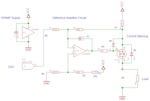
Then the complete circuit looks like this.

Good luck. Have fun.
Klaus
here I´d like to show how to design a DAC controlled high side constant current source
Often used as 0..20mA (or 4..20mA) current loop interface, thus we focus on the interface requirements.
* low speed ( maybe some 10Hz up to some kHz)
* high precision
* low drift
* high stability
* ruggedness
What do we need:
* power source: VCC, GND, Let´s say VCC = 12V
* DAC
* OPAMP
* MOSFET (you could use a PNP transistor, but base current causes an error in load current. Mosfet-gate current is about zero, thus the MOSFET solution is more precise)
* some Rs, Cs, Ds..
I decided to use a "difference Amplifier circuit", because it´s easy to calculate.

* Opamp Supply: every Opamp needs power to operate and it needs a capacitor to stabilize this power supply. 100nF close to the OPAMP is often a good value.
* Difference Amplifier Circuit: simple circuit: R1 = R3, R2 = R4, Gain = R2 / R1
Operation: It simply regualtes the Opamp_output in a way that (V_Feedback - V_OuptutRefernce) = gain x (V_NonInvertingInput - V_InvertingInput)
* DAC: use one with voltage output. This one has an output voltage range 0...5V
* MOSFET: P-Channel, no special one needed. Specifications are: Vcc, I_load, P_tot = VCC x I_Load. Add some headroom to every value.
Current Steering Circuit:
We want to regulate load current.
All load current goes through Mosfet_Drain and Mosfet_Source
..and thus it goes through the shunt (R5).
--> If we know the value of R5 and the voltage across R5 we know the load current.
(1) Thus we feed back (measure) the voltage across R5 to control the load current.
Varying the gate voltage will cause the load current to vary.
To make the P-channnel MOSFET (more) conductive: the voltage at the gate referenced to the source needs to go (more) negative.
(2) The feedback voltage is across R5. This means the feedback voltage is referenced to VCC. Thus we need to connect VCC to the OutputReference of the DifferenceAmplifierCircuit.
(3) The OPAMP_ouptut should control the gate of the MOSFET.
To avoid ringing it´s a good idea to connect OPAMP_output to Mosfet_gate with a resistor. The resistor value is not critical for this low speed application. We use 1kOhms.
(The higher the expected regulation speed the lower the resistor)
(4) The load is connected to Mosfet and GND
Now we need to decide how to connect the DAC:
Imagine: We want: The higher the DACOutputVoltage the higher the load current. And from above we know: The lower the gate voltage the higher the output current.
And because gate voltage = OPAMPOuptut voltage: The HIGHER the DAC voltage the LOWER the OpampOutput voltage. This is inverting operation.
(5) This tells us we need to connect the DACOutput to the InvertingInput
(6) And because the DACOutput is GND referenced we need to connect the NonInvertingInput to GND
Now to the device values:
Shunt: the current is 0..20mA. The voltage drop across the resistor should be large enough to get good measurable feedback voltage, but not too much, because it limits the voltage across the load. Let´s say 2V @ 20mA is a good compromise. --> R = V/I = 100 Ohms
R1, R2, R3, R4: High impedance may cause noise and reduces speed. Low impedance causes high current and thus it stresses the DAC output. For low DAC output current we choose a relatively high value resistor: 100k Ohms. (For sure one could use 10k for lower noise)
This is R1. But we know R3 = R1. Thus R3 is 100k, too.
To get the value for R2 and R4 we need to know the gain: |Gain| = |OutputVoltage / InputVoltage|.
Input voltage is the DAC voltage. 0..5V. Output voltage is the ShuntVoltage = 0..2V.
Thus gain = 2V / 5V = 0.4
Thus R2 = R4 = R1 x 0.4 = 40k (DifferenceAmplifierCircuit formula)
(For a real application I recommend to add some headroom and thus calculate wiith a of 10% higher load current: 22mA --> V_Shunt = 2.2V --> gain = 0.44 --> R2, R4 = 44k)
Now the circuit looks like this:

Improvements:
(7) Stability: The path from OPAMP_Output --> R7 --> MOSFET --> R5 --> R2 --> inverting input causes delay. This delay may cause instability, like ringing and continous oscillations.
To avoid this one adds a capacitor directly from OpamOutput to inverting input.
It forms a feedback with cutoff frequency that depends on the parallel circuit of R1||R2. (28k6)
For a 4..20mA loop a cutoff frequency of about 1kHz is a good value. thus C = 1/( 2 x Pi x f x R) = 5.6nF --> use a 4n7nF for C2
(The smaller the capacitor the higher the cutoff frequency, the faster the regulation response, but the higher the risk for instability)
(8) Limiting V_GS:
Especially with higher VCC there is the risk that V_GS of the MOSFET is exceeded by the OpampOutput. Thus a Zener diode is a simple solution to limit V_GS. Zener voltage needs to be less than the V_GS limit.
(9) Limiting V_DS:
Drain signal is the signal to the load. Thus it is expectable that can be touched by a user. (Maybe it is feed via connectors and cables...) Thus it is prone against ESD.
To protect the MOSFET against ESD we install a zener diode across the MOSFET. The Zener rating needs to be higher than VCC but lower than V_DS rating of the MOSFET.
(10) Improving PSRR: (power supply rejection ratio)
For a good DifferenceAmplifierCircuit R2 = R4. But in your case R2 is in series with the shunt. For precise regulation we need to take care about this. Otherwise a variation in VCC gives a variotion in I_Load. We could try to install a 39k9 resistor in the place of R2. But it may be hard to find.
The simpler solution is to add the shunt value (100 Ohms) to the R4 value.
This causes a small change in gain.
Then the complete circuit looks like this.

Good luck. Have fun.
Klaus
