Continue to Site

Welcome to EDAboard.com

Welcome to our site! EDAboard.com is an international Electronics Discussion Forum focused on EDA software, circuits, schematics, books, theory, papers, asic, pld, 8051, DSP, Network, RF, Analog Design, PCB, Service Manuals... and a whole lot more! To participate you need to register. Registration is free. Click here to register now.

Delaying Sample and Hold by one Clock cycle

Amr Wael

Member level 5
Member level 5
Joined
Jul 13, 2020
Messages
84
Helped
0
Reputation
0
Reaction score
1
Trophy points
8
Activity points
866
Hello ,
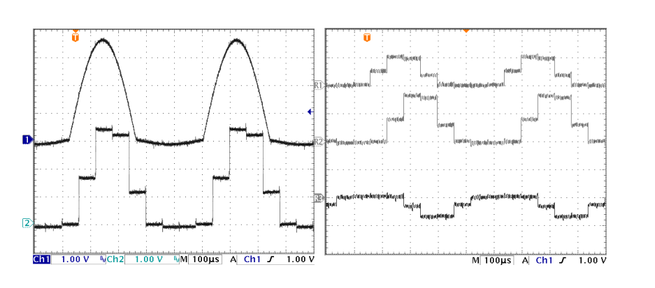
I am trying to implement a module that delays the clock of the sample and hold amplifier by one cycle in order to achieve the signals as in the following photo,
1709632632713.png

The photo on the left shows a rectified signal and a single sampled signal with a clock.

The photo on the right shows the regular sampled signal with the clock and the other two are sampled signals with delayed clock cycles ( 1 clock cycle for each signal)
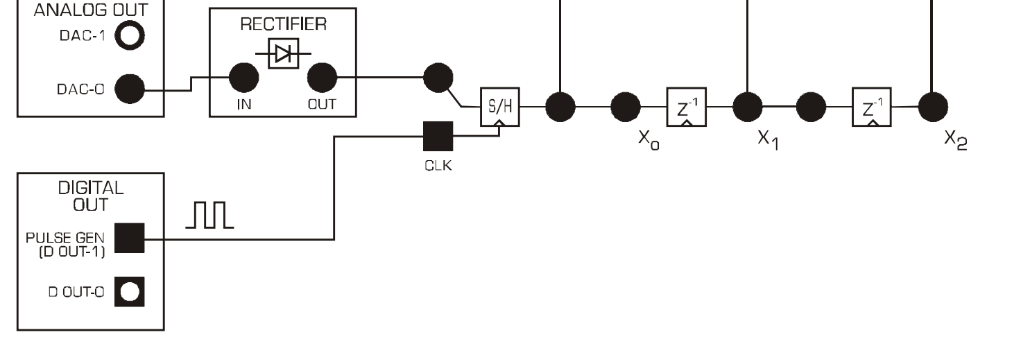
Here is a block diagram for what I am trying to do.
1709632761324.png

Note : Clock signal is delayed and is also input to Z-1 modules

I Tried using phase shifter based on opamp and RC to delay the clock 360 degrees before the other 2 sample and hold amplifiers but it didn't work.

Any solutions ?????

Thank you very much in advance.
 
HI,

are you sure you want to delay the clock?
I rather guess you want to delay the signal.
--> Please confirm.

****

I don´t understand your right picture:
* I expected the second (from top) waveform to have the same amplitude as the first signal
* I expected the third waveform to be identical as the second (and the first) wavefrom, but delayed.
.. but both does not match my expectations.

******

if you want to delay the signal by one complete clock period time, then I have this approach:
signal --> SH1 --> SH2 --> SH3 -->
while
* SH1 (you already have) is driven by positive clock
* SH2 is driven by inverted clock
* SH3 is driven by positive clock

Klaus
 
One possibility, PSOC SOC, one chip -

1709644994181.png


What else is onchip (multiple copies in most cases) :

1709645058593.png


Compiler and IDE (PSOC Creator) free, board ~ $20, CY8CKIT-059


1709645190529.png


Regards, Dana.
 
I’m with Klaus; your scope plots do not represent what you SAY you want. In the right hand picture the second signal looks like a delayed version of the first with a different amplitude. I have no idea what the third signal is.

I’m guessing (and this is really just a guess) what you REALLY want is to delay your analog signal by one clock. You could convert the signal to digital and delay it simply in the digital domain, but without knowing your ultimate goal, it’s just guessing. You could also use a bucket-brigade delay or a delay line. Who knows?
 
I think self-timed sampling is not going to give you the quality
(waveshape) you want, reliably. All the timing variation is going to
give you what you see, and slosh around with external influences
and internal variability.

Where transistors are free, the solution might be a PLL that syncs
to (say) positive zero crossing and generates however many samples
per cycle makes a "clean enough" modified sine wave.

What constitutes that, is your call.

Consider that your sine wave input might carry noise which spoofs
the trigger event and makes other kinds of mess. The PLL will act
as a "flywheel" in that respect.
 
For a discrete design, you are correct in that you need delayed sampling clocks from cascaded ring counter with a preload of 10000.. for however many delays you need from the master clk.

Each output must be Gated with a 1 shot sampling clock for RC to capture to 99% or 10T and not leak from input bias current between samples.

Only use NP0 ceramics or film caps to avoid hysteresis and microphonics.
 
I exaggerated the sample rate to show the delay (new scope could not figure out how to
get delayed sweep properly zoomed). Everything seems to work fine

1709662530232.png


And correct implementation :

1709662661830.png


Regards, Dana.
 
@KlausST @barry I would Like to delay the Clock signal (S/H Control) not the Input analog signal.
Analog signal is also delayed however as a result of delaying the clock signal.
Here is a photo to demonstrate what I am trying to do.
The only reply that's considered a solution for my problem is @danadakk but it's software solution , i could do it but still looking if it could be implemented hardware.
1709721312360.png
 
Curious, the problem for you with HW and SW solution is ?

I think it only took ~ 10 lines of code.......prior post.

A simpler approach :

1709723674078.png


You can do in HW using 2 S/H, a stable clock, this takes 2 lines of code to start the S/H's. Note they
are edge triggered. Delay is 5 uS in this case, 1/2 the period of the clock. If you dont use any other
part resources dont do this in PSOC, use 2 S/Hs, CMOS inverter, stable clock (so jitter does not
create S/H noise). Note using PSOC with just internal clock, I think that is accurate to +/- 4% if
absolute accuracy not a big problem, jitter < 2 nS. So PSOC would be a one part solution (ignoring
need for regulated supply which I am guessing you already have).

Why do you need this delay, I dont think you have commented on this....? What else in design
needs resources ?


Regards, Dana.
 
Last edited:
Hi,

this all makes no sense.

I would Like to delay the Clock signal
then your block diagram of post #1 shows everything else, but not a delayed clock:
If you want to focus on a delayed clock, then draw a delayed clock.

to delay the clock 360 degrees
delay a clock by 360°. What do you expect it to show? It´s exactly the same as the clock before.

Try it:
Look (with your eyes) at a point. Now turn yourself by 360°. What do you see now?

Klaus
 
@KlausST @barry I would Like to delay the Clock signal (S/H Control) not the Input analog signal.
Analog signal is also delayed however as a result of delaying the clock signal.
Here is a photo to demonstrate what I am trying to do.
The only reply that's considered a solution for my problem is @danadakk but it's software solution , i could do it but still looking if it could be implemented hardware.
View attachment 189193
If you delay a clock by one cycle it looks EXACTLY THE SAME!! I think you are confusing a CLOCK with a non-continuous S/H control.

maybe you want to delay your SH control signal, which is not a clock, but a single pulse? delay it relative to what?

Your original picture shows a delayed SIGNAL, not a delayed CLOCK.
 
Your time delayed samples seem to indicate delayed signals being sampled by the same clock as in a "bucket brigade" once implemented that was long ago implemented in a cascaded charge in a series of charge coupled devices.

Each 1/8f time delay there may be sampling residue or crosstalk (memory) injected into the sampled signal. Cascaded, the noise will add to the sampled signal unless properly isolated.

Your bottom trace is perhaps in error shown in inverted polarity with an additional 1/8f delay and 1/2 scale.

This cannot be created by 1 clock and 1 inverted clk. and must be created 3 cascaded sample clocks that do not overlap the setup and hold time of your S&H circuit.

i.e. the outputs are cascaded S&H values from the top down but the sample sequence must be from the bottom up such that the lowest trace gets the oldest delayed sample and the top trace samples the raw input.

The delayed pulses only need to be delayed more than the pulse width of the Sample pulse width to avoid a metastable condition where 2 consecutive stages yield the same result.

1709741500318.png


There are other methods using SPDT with track and hold
- most ceramic caps will display glitches from memory effects due to dC/dV + hysteresis
 
Last edited:
Hi,

Are you processing the clock prior to its use for the sampling (e.g. is your application enabling the clock for some clock cycles and disabling the clock for some other clock cycles? It's in situations like that that delaying the clock could be useful. If the clock is constantly running, then it wouldn't be useful delaying it.
 
Here is project using the S/Hs to do the job.

2 Khz sine, delay ~ 4 uS, Pin_0_7 and P_0_6 output pins. P_0_0 output of WaveDAC.

3 lines of code in main(), just to start the wavedac and the 2 S/H's

1715277237042.png


Project attached. Unzip (it will gen a folder) and dbl click the .cydwr file or open file from within Creator.


Regards, Dana.
 

Attachments

  • One Clock Delay using Sample Holds.cywrk.Archive01.zip
    1.6 MB · Views: 52

LaTeX Commands Quick-Menu:

Similar threads

Part and Inventory Search

Welcome to EDABoard.com

Sponsor

Back
Top