Hi there. I am having a go at this. I might be wrong though.
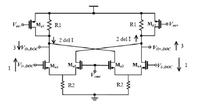
From your figure 1 it looks like they have assumed a positive offset in the left arm and negative offset in the right arm
Figure 1:


The numbers in the figure indicate the order in which the direction of the voltage/current varies. As you can see if we have an offset in the direction given (1), the current changes in the direction given (2) which results in change in the output voltage in the direction given (3).
After the amplifiers A1,A2 and A3 we have a feedback network (see the naming convention that I have used in the figure below)
Figure 2:


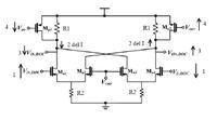
This will change the control voltages in the below figure in the direction given (4)
Figure 3:


So that the changes in del I current gets compensated and the current through the resistors R1 goes towards its original value and thereby the output voltages of amplifier A1 also go towards its orginal values. But where does it stop? It stops when the complete feedback path in figure 2 is valid. If A2 and A3 are large enough, ΔVout in figure 2 will settle at the control voltage so that ouput voltages of A1 is very small (which depends on the A2A3 gain). In order to have a very less ΔVout we should have the gain A2A3 and the offset transistor Mp1 and Mp2 (decides the offset gain) to be huge.
The RC filter in the feedback network is there for allowing only dc (offset is a dc phenomenon) and doesn't allow the signal (which is the input to the VGA and can have a very high frequency) to alter the offset control voltages. By this way we ensure that the signal doesn't affect the offset control voltages.
The common mode is chosen in the midpoint of the input common mode range so that you get maximum swing on either sides. The output common mode range is decided by the input common mode and the ratio of two resistors R1 and R2. Let's say there was no offset cancellation network. The current through R1 is
\[
I_{R2}=\frac{V_{cm_{input}}-V{gs_{n1,n2}}}{R2}
\]
\[
V_{cm_{output}}=I_{R2}R1=(V_{cm_{input}}-V{gs_{n1,n2}})\frac{R1}{R2}
\]
Can you just mention the paper title if possible?


