Continue to Site

Welcome to EDAboard.com

Welcome to our site! EDAboard.com is an international Electronics Discussion Forum focused on EDA software, circuits, schematics, books, theory, papers, asic, pld, 8051, DSP, Network, RF, Analog Design, PCB, Service Manuals... and a whole lot more! To participate you need to register. Registration is free. Click here to register now.

[SOLVED] dc-dc boost converter-mosfet getting damaged

Status
Not open for further replies.

sabu31

Advanced Member level 1
Joined
Jan 28, 2011
Messages
467
Helped
12
Reputation
24
Reaction score
13
Trophy points
1,298
Activity points
5,359
Hi
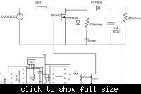
I had made a dc-dc boost converter. I/p 150V, O/p 375V , load=450ohms. The gate driver is IXDN504PI. However when i tested the converter at the rated voltage the switch blew off after 2-3 min. The heat sink was just warm and not very hot. The switch i used was IRF840 (500V,8A).There was no ringing effect, the voltage spike during turn off was 25 volts for 200ns. The output diode also got damaged as well as the gate driver IC. I had used back to back zeners(15v) at gate terminal for protection. I have two questions
1) What should be the switch rating(or safety margin) so that it can be used for o/p 400V at nearly 350W continuously say for 8-10hrs.Is IRF840 enough?
2) What should i do for the driver protection in case the switch gets damaged. I came across article where back to back zener was used for protection , however here the zener was not effective.

Thanking you
 

back-to-back Zener (or better known as TSV Transient Voltage Suppressor) is intended more for high-voltage spike, ESD and impulse ultra-shock etc.
In your case, it can help as protection device.
Advice is to check the datasheet for the suitable Zener/TSV that can absorb the energy that kicks in, as using the right Zener can do a good and effective job too.

Switch rating should be at least 20% higher than your operating limit. Industrial practice cater 20% to 50%, depending the system requirement.

I wonder how you connected your switch. Would be helpful if you post your circuit diagram.

Hi

Thanks for the reply. I am driving the switching using IXDN504PI, using 10 ohm gate resistor. NOw when i checked i found that gate resistor has changed its value to nearly 1K(in other words, it also got damaged). Also the zeners are damaged. I used quater watt zener(15V).
Since the drain voltage would be around 400V, what should be the rating of zener for of protecting the gate driver IC. Secondly, always whenever the switch is damaged, the output diode of the boost converter aslo gets damaged.why does this happen.I have posted the image of circuit.


If the boost diode failed in your blow up - then it must have failed FIRST. Otherwise if the fet failed first the diode would be unaffected - you need a better boost diode!
Having looked at the spec sheet for this diode - it is far too slow for this application and will overheat and die every time...
Regards, Orson Cart.
 
Last edited:
  • Like
Reactions: sabu31

    sabu31

    Points: 2
    Helpful Answer Positive Rating
The failure pattern suggests a drain-gate breakdown, feeding high voltage to the gate node. I wonder, if it's reasonable to protect the gate driver in this situation.

I don't see a particular reason for the observed problems. A problematic point is the inverting characteristic of the optocoupler output, that switches to on, if the LED current is missing. This may easily cause fatal damage. I also wonder, if you can be sure, that the control circuit won't ever generate a too high duty cycle. I would personally prefer current mode control of the boost converter or at least a overcurrent shut-down feature.

If the boost diode failed in your blow up - then it must have failed FIRST. Otherwise if the fet failed first the diode would be unaffected.
I'm not sure about. If the FET switches off with a high overcurrent, both devices may be damaged instantly.

P.S.:
Having looked at the spec sheet for this diode - it is far too slow for this application and will overheat and die every time...
Surely a possible explanation. But nothing has been said about switching speed yet. The LC dimensioning rather looks like low kHz which won't be a problem.
 
Last edited:

Hi
Thanks guys for the input.
I am using the converter at 50Khz. The reason i am using this high value of capacitor is that, this stage is supposed to be input to inverter(dc-link capacitor, to reduce ripple of inverter output). I am at present testing it in open loop so no damaged due to defective control.Also regarding that opto inverting characteristic (if i use IXDI504PI inverting output,that problem could be solved).
Secondly the diode which i used is PFr856 which has Trr of 200ns, would that be sufficient at 50Khz? Also current rating of diode is 3 A, at 370 W output and 400V , the load/diode current would be nearly 1A so its not going above diode rating.

SO again it comes back to question a) why is switch and diode getting damaged together b) how to protect the gate driver ic.

---------- Post added at 15:17 ---------- Previous post was at 14:11 ----------

Hi
Thanks guys for the input.
I am using the converter at 50Khz. The reason i am using this high value of capacitor is that, this stage is supposed to be input to inverter(dc-link capacitor, to reduce ripple of inverter output). I am at present testing it in open loop so no damaged due to defective control.Also regarding that opto inverting characteristic (if i use IXDI504PI inverting output,that problem could be solved).
Secondly the diode which i used is PFr856 which has Trr of 200ns, would that be sufficient at 50Khz? Also current rating of diode is 3 A, at 370 W output and 400V , the load/diode current would be nearly 1A so its not going above diode rating.

SO again it comes back to question a) why is switch and diode getting damaged together b) how to protect the gate driver ic.

Hi
I just now tested the converter at 75V i/p and op=150V, the output diode got heated very rapidly(didnt check o/p diode temperature before). I think the diode must have blown up before mosfet,But what could be the reason for the diode to get heated up. Is it current spikes during switching .
 

Which is your load in your circuit? Is it the 450 Ohm?
It would be good if you label the ratings for the components used to ease troubleshooting.

Could you scale down your design to 10V, so you reduce the risk of damaging those devices?
In this way, you can also gradually step up your voltage to 30V, 50V 70V etc and perform measurements at strategic nodes.
Sometimes this way you can narrow down and identify devices that fail.

To protect switch, use a flywheel diode.

Switch and diode both got damaged either the current exceeded the ratings. Would be better if you do a scale down version of your circuit and step up to see better.

Hi
SO again it comes back to question a) why is switch and diode getting damaged together b) how to protect the gate driver ic.
 

Hi

The 450 ohm is the load, which is to be used at 400V (under test conditions). However even when the o/p voltage is 150V, ie 0.33 A current... the o/p diode is getting heated very much after a minute or so..
 

For 50 kHz switching frequency, I completely agree with Orson's analysis. The excessive diode heating will be mainly generated by switching losses.
 
  • Like
Reactions: sabu31

    sabu31

    Points: 2
    Helpful Answer Positive Rating
For the diode leading to the 450 Ohm load, you may want to consider a Schottky diode. If you are using 1A, perhaps go for 1.5A or 2A rating.

For the diode leading to a shunt capacitor, is it a recommended to use in the reference design of the switch?

Hi

The 450 ohm is the load, which is to be used at 400V (under test conditions). However even when the o/p voltage is 150V, ie 0.33 A current... the o/p diode is getting heated very much after a minute or so..
 

Re: dc-dc boost converter-diode failure

There is a simple way to show that it is the diode failing and not the mosfet, start & run the circuit run normally and then (within a few seconds) command the mosfet to 100% ON (no off time) pretty soon the fet will fail due to overcurrent (make sure there is a sensible fuse on the supply to the circuit) - after the failure - check the diode - it will be fine - Regards, Orson Cart. p.s. at high temp and 50kHz this diode has very poor switching action and high losses
 

Re: dc-dc boost converter-diode failure

Thanks guys for the reply. I am going test by replacing the o/p diode by SiC schottky diode,however it has Qc=122nC. Hope that doesnt create problems..
Also i wanted to know regarding the power rating of the back to back zener to be used for protecting gate driver. Any references would be helpful.. Thanks
 

Also i wanted to know regarding the power rating of the back to back zener to be used for protecting gate driver.
You'll find exact pulse power ratings for dedicated TVS diodes. Standard Z-diodes still have considerable pulse power handling, but factor 10 to 100 below TVS diodes. Check the data sheets, NXP BZV55 e.g. has detailed data.
 

Status
Not open for further replies.

Similar threads

Part and Inventory Search

Welcome to EDABoard.com

Sponsor

Back
Top