Darligton Pair Bandwidth - BC550 transistors
- Thread starter ironman88
- Start date
- Status
- Not open for further replies.


- Joined
- Jan 22, 2008
- Messages
- 53,715
- Helped
- 14,812
- Reputation
- 29,921
- Reaction score
- 14,447
- Trophy points
- 1,393
- Location
- Bochum, Germany
- Activity points
- 303,670
Bandwidth must be defined referring to a specified amplifier circuit.
A product of bandwidth numbers makes no sense in any case.
A product of bandwidth numbers makes no sense in any case.

esp1
Advanced Member level 1

hi 88,
The maximum frequency of a transistor is quoted as Ft.
The BW is function of the overall amplifier circuit configuration and gain requirement.
Do you have a circuit design in mind.?
E
The maximum frequency of a transistor is quoted as Ft.
The BW is function of the overall amplifier circuit configuration and gain requirement.
Do you have a circuit design in mind.?
E
ironman88
Newbie level 3

hi 88,
The maximum frequency of a transistor is quoted as Ft.
The BW is function of the overall amplifier circuit configuration and gain requirement.
Do you have a circuit design in mind.?
E
First of all thanks for your replies,
basically I have in mind an amplifier which first amplifies a photodiode current trhough a darligton pair, then I use two stages of collector follower amplifier to convert the signal in a sufficient voltage level for further processing and I am trying to see how it is possible to make an estimation of a darligton pair bandwidth

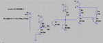
The input current pulse is a 2.8MHz ~mA pulse which simulates the current response of the photodiode and this is implemented with a BJT component.
Last edited:
esp1
Advanced Member level 1
hi 88,
If that posted circuit was created using LTSpice, you could use LTSpice to display the BW.
Post your LTS asc file and I will run a Sim.
E
If that posted circuit was created using LTSpice, you could use LTSpice to display the BW.
Post your LTS asc file and I will run a Sim.
E
godfreyl
Advanced Member level 5
Nevermind bandwidth. The circuit won't work as shown. One way to fix it is to connect the collector of Q1 to +5V, instead of to the collector of Q2.
esp1
Advanced Member level 1
hi godfreyl,
Q1 to Q2 collector is a correct connection for a Darlington pair.
If he connects Q1 collector to +5V there is nothing to limit the current thru Q1 and the Base/Emitter of Q2.
E
Q1 to Q2 collector is a correct connection for a Darlington pair.
If he connects Q1 collector to +5V there is nothing to limit the current thru Q1 and the Base/Emitter of Q2.
E
godfreyl
Advanced Member level 5
OK, but the problem remains:
What he wants is that when Q1 and Q2 switch on, they switch off Q3.
But that won't work because the voltage on the collector of Q1 can't go low enough, Q1 will saturate.
What he wants is that when Q1 and Q2 switch on, they switch off Q3.
But that won't work because the voltage on the collector of Q1 can't go low enough, Q1 will saturate.
- Joined
- Jan 22, 2008
- Messages
- 53,715
- Helped
- 14,812
- Reputation
- 29,921
- Reaction score
- 14,447
- Trophy points
- 1,393
- Location
- Bochum, Germany
- Activity points
- 303,670
In the present circuit there's no reasonable purpose of a darlington stage. It can be also expected that the circuit behaviour will be dominated by other transistor parameters than ft, e.g. switching delay caused by charge storage.
ironman88
Newbie level 3
Hi,
I know how to get the BW by ltspice but I do not know to describe it in terms of theory (for Darligton pair),
by the way I am getting a 2.8MHz 0 to 5 V square pulse as desired (output) what is the main problems you suggest?
the first BJT is supposed to simulate the current produced by photoreceivers which receive a pulsed signal the rest of the amplifier functions like a transimpedance amplifier
esp1
Advanced Member level 1
hi 88,
If you post your LTS circuits 'asc' file I will run the Sim, then we we can discuss the problems using a common reference.
If the site software does not allow 'asc' file uploads, change the file extension to .txt.
E
If you post your LTS circuits 'asc' file I will run the Sim, then we we can discuss the problems using a common reference.
If the site software does not allow 'asc' file uploads, change the file extension to .txt.
E
- Status
- Not open for further replies.
Similar threads
-
-
Astable multivibrator using 555 vs transistors
- Started by ay215
- Replies: 9
-
-
How to calculate differential pair target Zdiff?
- Started by Rimvis123
- Replies: 12
-