Continue to Site

Welcome to EDAboard.com

Welcome to our site! EDAboard.com is an international Electronics Discussion Forum focused on EDA software, circuits, schematics, books, theory, papers, asic, pld, 8051, DSP, Network, RF, Analog Design, PCB, Service Manuals... and a whole lot more! To participate you need to register. Registration is free. Click here to register now.

Current Mirror Layout with Interdigitation

goatmxj666

Member level 3
Member level 3
Joined
Mar 5, 2023
Messages
54
Helped
0
Reputation
0
Reaction score
1
Trophy points
8
Activity points
513
Hello.

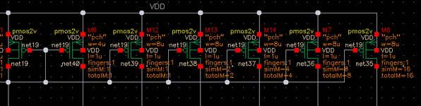
I am currently doing the current mirror layout.

The sizes of each are as follows.
1722916961755.png

I would like to layout with interdigitation method for matching. I think common centroid layout is not possible as it is too time consuming.

Also, I made some of the mosfets 8um because it was too long to do all the mosfets in 4um.

I was thinking of doing something like "D D D D D D D D D D D D D D C C C C C B B A F E G A B B C C C C C D D D D D D D D D D D D D", is that okay?

I really need some advice from layout experts.

Any advice would be greatly appreciated.

Thanks.
 

Attachments

  • 1722916803110.png
    1722916803110.png
    11.2 KB · Views: 56
Solution
What I understand is that create finger pairs from "D D D D D D D D D D D D D D C C C C C B B A F E G A B B C C C C C D D D D D D D D D D D D D" and then arrange them in the order of DCBAFEGABCD. Is this correct?
1. Your array is probably too big for a single-line interdigitation pattern (the aspect ratio of the array would be too large which is bad for gradients);
2. Keep at least 2 fingers for each device;
3. Keep the same unit width for each transistor (use multipliers to achieve target total width);

My idea of device sizing and matching is attached. It's somewhere in between of common-centroid and interdigitation, but it passes the gradient test, so it should be okay. Consider using Layout GXL for faster device placement...
You're probably already overthinking it but one recommendation is to make every "finger" a finger-pair to make full low level symmetry, then distribute those pairs as you see fit.

Until you get to very large W*L, random mismatch is likely to still dominate any gradient driven "anecdotally systematic" (thermal, alignment) offset contributions.
Especially at finer nodes with RDF now a thing.
Hello. Thank you so much for your answer.

What I understand is that create finger pairs from "D D D D D D D D D D D D D D C C C C C B B A F E G A B B C C C C C D D D D D D D D D D D D D" and then arrange them in the order of DCBAFEGABCD. Is this correct?
 
What I understand is that create finger pairs from "D D D D D D D D D D D D D D C C C C C B B A F E G A B B C C C C C D D D D D D D D D D D D D" and then arrange them in the order of DCBAFEGABCD. Is this correct?
1. Your array is probably too big for a single-line interdigitation pattern (the aspect ratio of the array would be too large which is bad for gradients);
2. Keep at least 2 fingers for each device;
3. Keep the same unit width for each transistor (use multipliers to achieve target total width);

My idea of device sizing and matching is attached. It's somewhere in between of common-centroid and interdigitation, but it passes the gradient test, so it should be okay. Consider using Layout GXL for faster device placement (you can enter your pattern there).
Good luck!

P.S. Even though the array looks massive, when you will stack the neighboring MOSFETs, I think it should be fine :)

IMG_8022.JPEG
 
Solution
1. Your array is probably too big for a single-line interdigitation pattern (the aspect ratio of the array would be too large which is bad for gradients);
2. Keep at least 2 fingers for each device;
3. Keep the same unit width for each transistor (use multipliers to achieve target total width);

My idea of device sizing and matching is attached. It's somewhere in between of common-centroid and interdigitation, but it passes the gradient test, so it should be okay. Consider using Layout GXL for faster device placement (you can enter your pattern there).
Good luck!

P.S. Even though the array looks massive, when you will stack the neighboring MOSFETs, I think it should be fine :)

View attachment 193102
Thank you for your very detailed and thoughtful response. It really helped me a lot.
 

LaTeX Commands Quick-Menu:

Similar threads

Part and Inventory Search

Welcome to EDABoard.com

Sponsor

Back
Top