Continue to Site

Welcome to EDAboard.com

Welcome to our site! EDAboard.com is an international Electronics Discussion Forum focused on EDA software, circuits, schematics, books, theory, papers, asic, pld, 8051, DSP, Network, RF, Analog Design, PCB, Service Manuals... and a whole lot more! To participate you need to register. Registration is free. Click here to register now.

CTAT voltage generator

Status
Not open for further replies.

celebrevida

Member level 2
Member level 2
Joined
Oct 25, 2016
Messages
47
Helped
0
Reputation
0
Reaction score
2
Trophy points
8
Activity points
524
I am trying to design a CTAT voltage generator such that:
Vout = mx + b
where I can control both m and b separately.
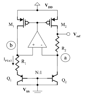
bvr.png


The closest I can come up with is using the CTAT voltage of a bandgap reference circuit.
If R2 is actually several transistors in series, then I can select different taps "inside" R2 using an analog mux and thus select slope "m".

And we can see that:
  1. Node (a) would have the most negative slope (m_maxneg)
  2. Node Vref would have a flat slope. (m_0)
  3. All nodes between Vref and a would have a slope between m_0 and (m_maxneg).
The issue is that while this works for selecting "m", it doesn't work for selecting "b".
As I select the slope "m", I am also changing "b" at the same time!

How can I design a CTAT voltage reference in which both "m" and "b" are independently selectable?

Thanks for any help!
 

Hi,

Probably haven't understood several points...

What about separating a and b off from each other by duplicating the shown schematic so one handles a, the other handles b, and these are summed by a third OA, or something along those lines?
 

This can get tricky.
You can control the "m" by changing the values of the resistors used as you have observed.
Regarding the "b" part, as it is evident, "b" is a constant which is independent of the temperature. Which would mean that you would need to generate a constant voltage and then sum it with the desired CTAT.
So technically a BGR followed with a summing amplifier.
 

If you can stand some granularity then put MOS switches in both the PNP nest (say, enable {4,6,8,...}:1) - maybe making each segment include its tail (TC) resistor - and also the PTC resistor R2. Each is now a DAC, have yourself a time.
 

Thanks for all replies.

After thinking about the easiest way to do this the best I can come up with is:

Use the BGR to generate the PTAT voltage, select points inside "inside" the R2 resistor to select the slope. Of course this selects both the slope and the intercept at the same time!

Then use Vptat as the reference to a LDO regulator with variable feedback to generate the final Vout. In essense, shift the Vptat up or down.

Doing it this way, you can't truly adjust the slope and the intercept independently. However it's a lot easier than trying to use complex circuitry to add or subtract the "slope" from a fixed Vref.
 
Status
Not open for further replies.

Similar threads

Part and Inventory Search

Welcome to EDABoard.com

Sponsor

Back
Top