Max01800
Junior Member level 2

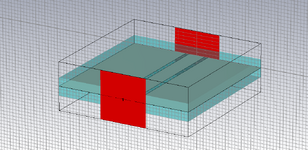
Hey guys, I'm trying to simulate a CPW sandwiched between two dielectric substrate, as shown in the photo. There are two Waveguide Port and I put open boundaries on all the faces of the boundary box. During the simulation I get this warning
"Waveguide port x touches transversal open boundary"
1) What does it mean?
2) Should I be worried?
3) How do i solve this? Which boundary should I use?
"Waveguide port x touches transversal open boundary"
1) What does it mean?
2) Should I be worried?
3) How do i solve this? Which boundary should I use?