Continue to Site

Welcome to EDAboard.com

Welcome to our site! EDAboard.com is an international Electronics Discussion Forum focused on EDA software, circuits, schematics, books, theory, papers, asic, pld, 8051, DSP, Network, RF, Analog Design, PCB, Service Manuals... and a whole lot more! To participate you need to register. Registration is free. Click here to register now.

Create layout directly in Allegro PCB SI

Status
Not open for further replies.

pavel47

Member level 4
Member level 4
Joined
Nov 8, 2005
Messages
68
Helped
0
Reputation
0
Reaction score
0
Trophy points
1,286
Location
Switzerland
Activity points
1,790
Hello,

Is it possible to create layout directly in Allegro PCB tool (without having a deal with schematic):

  • create list of nets
  • create geometry objects
  • associate these objects with nets
  • create stackup
  • associate particular net with a stackup layer

Thanks in advance

Pavel
 

Hi
you can keep the footprint and you can assign the net but it is not right method.
for assign net manually for footprints use this link

if you are using allegro please use this link
https://community.cadence.com/cadence_technology_forums/f/27/t/23175

which tool r u using better follow the design flow it will help for tracking in critical conditions
 

Yes but only if you are daft, the whole point of a schematic (circuit diagram) is to have a guide to the electronics, not only that but you are likely to add errors and updates will be impossible.
WHY do something the way we had to in the late 80's, it nearly 30 years since I didn't use a schematic capture package to enter the circuit diagram!
 

Pavel47, all schematic/layout packages will let you make a PCB without a schematic and many people use them this way for simple pcb's.
 

Simple PCB or not it is a rather silly way to work (and not many work that way, and those that do are DIYers), you have to have some form of schematic for your design, be it on paper or electronic, so you might as well enter the schematic electronically and get all the benefits and avoid the numerous pitfalls of adding connections within the PCB package or manually translating the schematic to a net list.
 

Simple PCB or not it is a rather silly way to work (and not many work that way, and those that do are DIYers), you have to have some form of schematic for your design, be it on paper or electronic, so you might as well enter the schematic electronically and get all the benefits and avoid the numerous pitfalls of adding connections within the PCB package or manually translating the schematic to a net list.

Hi Marce,

Thank you for feedback. The reason to use layout tool without schematic is to simulate a particcular structure from the elctromagnetic point of view: calculate mutual capacitance between conductors, or even better - extract spice model of structure in form of RC-matrix and then use it in circuit simulation.

The final goal is to simulate strcuture in Sigrity PowerSI 3D EM Full-Wave, but it seems that this tool can only import layouts.
So I see the flow in the following way:

  • create structure in PCB Editor
  • import it in Sigrity PowerSI
  • simulate strcuture using Sigrity 3D EM Full-Wave simulator
  • extract model spice in form of RC-matrix
  • use this model in overall circuit simulation

I would be grateful for any comments concerning this flow

Regards

Pavel
 

I use Si software and it is the same, you have to import a physical layout, but we do generate this from a schematic... Again it is the quickest and most error free way to do this.
What I can do is create scenarios in my SI tool, where I can pick a receiver and transmitter and then add transmission lines etc between them, but my tool is Cadstar SIV .

Hello Marce,

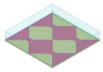
Is your tool capable to simulate the structure like this (please, see the picture)
there are 2 layers of conductors - dimond-like shapes and 2 ... 5 layers of dielectrics.
There is no schematic for such structure ... at least it isn't necessary at all ... ok I could deliberately create some schematic if layout tool does requires it ...
I've just tried with PowerSI and found a bizarrerie: tool doesn't allow to create shapes of signal-type layer ... only on plan layer.
Is Cadstar more flexible in this sens ?

Regards

3d_structure.JPG
 

Status
Not open for further replies.

Part and Inventory Search

Welcome to EDABoard.com

Sponsor

Back
Top