Continue to Site

Welcome to EDAboard.com

Welcome to our site! EDAboard.com is an international Electronics Discussion Forum focused on EDA software, circuits, schematics, books, theory, papers, asic, pld, 8051, DSP, Network, RF, Analog Design, PCB, Service Manuals... and a whole lot more! To participate you need to register. Registration is free. Click here to register now.

Coupling Method for Cavity Resonator

Status
Not open for further replies.

Ahmedsalim789

Junior Member level 1
Joined
Apr 9, 2015
Messages
19
Helped
1
Reputation
2
Reaction score
0
Trophy points
1
Activity points
140
Hi
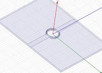
I designed a cylindrical cavity resonator but the structure is not resonating. I used the idea of microstrip line for excitation through two wave ports.
As another option for excitation of cavity resonator, I thought to place a patch of Copper on top side of cavity and this patch is given an inset feeding. But It did not work yet.

Please help me.
Thanks
 

Attachments

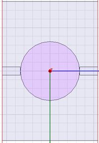
  • Top View.JPG
    Top View.JPG
    42.7 KB · Views: 144
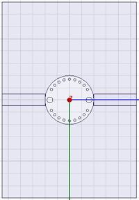
  • Top View_Inset Feeding excitation.JPG
    Top View_Inset Feeding excitation.JPG
    27.7 KB · Views: 153

Hi
I designed a cylindrical cavity resonator but the structure is not resonating. I used the idea of microstrip line for excitation through two wave ports.
As another option for excitation of cavity resonator, I thought to place a patch of Copper on top side of cavity and this patch is given an inset feeding. But It did not work yet.

Please help me.
Thanks

What mode is used?
 
TE(011) mode for cylindrical cavity is used, while frequency used is 2.4 GHz. I calculated dimension of cavity (radius and height) but they appear too large to fabricate. (For example radius appeared 80 mm and height was 160 mm, as I assumed height is equal to twice the diameter).

I am using Duroid/Rogers 5880 with standard thickness (1.575 mm). Any design suggestion or reference article, or dimension of cavity for my case, please let me know. Thanks.
 

Do you mean dielectric resonator (not cavity resonator)?

Then this might help:
**broken link removed**
http://www.trans-techinc.com/products_detail.asp?ID=11&Name=Dielectric-Resonators

A hole is drilled in the Duroid, and different samples are planned to test (for example, air filled, or liquid filled, or Teflon filled hole). Yes, in that sense it should be called dielectric resonator. Sorry, I was using the formulas of simple cylindrical cavity resonator.

- - - Updated - - -

 
Last edited by a moderator:

My designed structure is resonating properly (I checked through combined graph of real and imaginary impedance values). However two issues are still left to solve.
1) Structure was designed/expected to resonate at 2.4 GHz, but its resonance is occurring at 5.8 GHz.
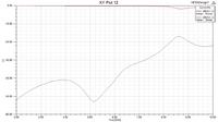
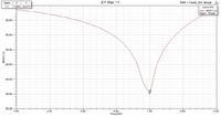
2) S parameters (S11, and S21) are very out of shape (Please have a look).
Any suggestion?
 

Issue is resolved now and S parameters are also in good shape.
Thanks.
 

Hello again,
I mistakenly mixed the idea of cavity resonator with dielectric resonator due to some confusion.
My intention is to design "Cylindrical Cavity resonator" without any dielectric filled inside cavity, which means cavity is empty (or filled with air).
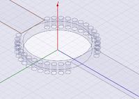
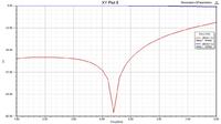
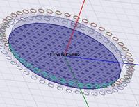
I have attached the following figure, the structure is resonating in a good way, however due to losses S parameters graphs are not in good shape. Any suggestion?


- - - Updated - - -

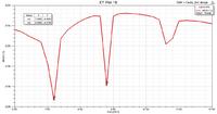
Please check the S21 curve:


- - - Updated - - -

I just did theoretical calculation (using Pozar's book formulae) and once again I got the same results: radius of cavity 82 mm, height of cavity 164 mm @ 2.4 GHz and using TE (011) mode.

While available substrate thickness is 1.575 mm in my laboratory, how it is possible to design it?
Please guide me, I doubt something wrong calculation or misunderstanding somewhere?
 

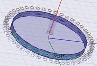
Where is your metal cavity? It is difficult to understand what you have designed. A hole in the substrate surrounded by smaller holes?

And your S-parameters look like a simple thru-line, not like a resonator, not like the structure that you have shown/drawn.
 

Where is your metal cavity? It is difficult to understand what you have designed. A hole in the substrate surrounded by smaller holes?

And your S-parameters look like a simple thru-line, not like a resonator, not like the structure that you have shown/drawn.

Yes, you are right, I failed to understand the meaning of "Air filled cavity". Now I modified the design in this way:
1) A hole is realized in the substrate by subtracting a cylinder.
2) A cylinder of same dimension (diameter and height) as of hole, is drawn to model the air material inside cavity. The curved walls and bottom surface of it is selected as Copper (Finite conductivity). Is this correct modeling of metallic cavity?

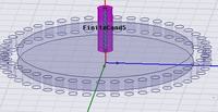
3) Coaxial feeding is employed at the center of the cavity, however I am confused whether inner cylinder of coaxial connector should touch the bottom surface of cavity or should it be bit above the bottom surface?

4) Another major drawback (in fact mistake) of my design is, changing the diameter of cavity is not affecting the resonant frequency, and it is staying at 21-24 GHz whatever changes I do with my design. It seems some serious mistake in my design. Please help me!


2) A cylinder of same dimension (diameter and height) as of hole, is drawn to model the air material inside cavity. The curved walls and bottom surface of it is selected as Copper (Finite conductivity). Is this correct modeling of metallic cavity?

I understand that you have no metal top cover.
Typically, the cavity is completely enclosed by metal (metallic box).

3) Coaxial feeding is employed at the center of the cavity, however I am confused whether inner cylinder of coaxial connector should touch the bottom surface of cavity or should it be bit above the bottom surface?

You want to create an electric field maximum in the resonator center. See diagram 2 here:
https://www.daenotes.com/electronics/microwave-radar/excitation-methods-of-cavity-resonator
 
I understand that you have no metal top cover.
Typically, the cavity is completely enclosed by metal (metallic box).


You want to create an electric field maximum in the resonator center. See diagram 2 here:
https://www.daenotes.com/electronics/microwave-radar/excitation-methods-of-cavity-resonator

Right, I agree.
Previously I made assigned "Finite conductivity" to the top of cavity, but it was overlapping with Upper ground layer, so i removed the finite conductivity of top of cavity.
(The substrate is middle layer, while top and bottom layers are grounded metal).
But I try to think in the direction as you said.
 

Now cavity consists of all sides of metal (top, bottom, and circular walls), a copper post is placed at the center of the cavity, and connected by inner cylinder of coaxial connector. Much better results now.
However, cavity diameter, and post dimension (diameter and height) are not affecting the resonant frequency. Any suggestion?


Near zero S11 response is appearing. Is it due to mismatch problem? A coaxial connector is used to feed a cavity resonator (ideal position at cavity center).

S11 is almst approaches to zero, which is completely wrong. Should I try to find suitable position across the surface of cavity for feeding point?
 

S11 is almst approaches to zero, which is completely wrong.

Is it wrong?

I think this is what we expect for such a resonator: almost total reflection outside the resonance. At resonance, reflection depends on the coupling to the resonator: it might be too weakly coupled.

If you visualize the E field, does that look correct (desired mode?)
 

Is it wrong?

I think this is what we expect for such a resonator: almost total reflection outside the resonance. At resonance, reflection depends on the coupling to the resonator: it might be too weakly coupled.

If you visualize the E field, does that look correct (desired mode?)

No, I did not check the E field yet. Yes, you are right, it's coupling is not correct (due to just randomly placed).
 

Status
Not open for further replies.

Part and Inventory Search

Welcome to EDABoard.com

Sponsor

Back
Top