Continue to Site

Welcome to EDAboard.com

Welcome to our site! EDAboard.com is an international Electronics Discussion Forum focused on EDA software, circuits, schematics, books, theory, papers, asic, pld, 8051, DSP, Network, RF, Analog Design, PCB, Service Manuals... and a whole lot more! To participate you need to register. Registration is free. Click here to register now.

Conformal LEC checking problem

Sameerpy

Newbie level 5
Newbie level 5
Joined
Mar 20, 2024
Messages
10
Helped
0
Reputation
0
Reaction score
0
Trophy points
1
Activity points
159
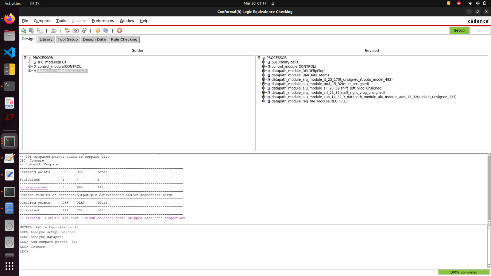
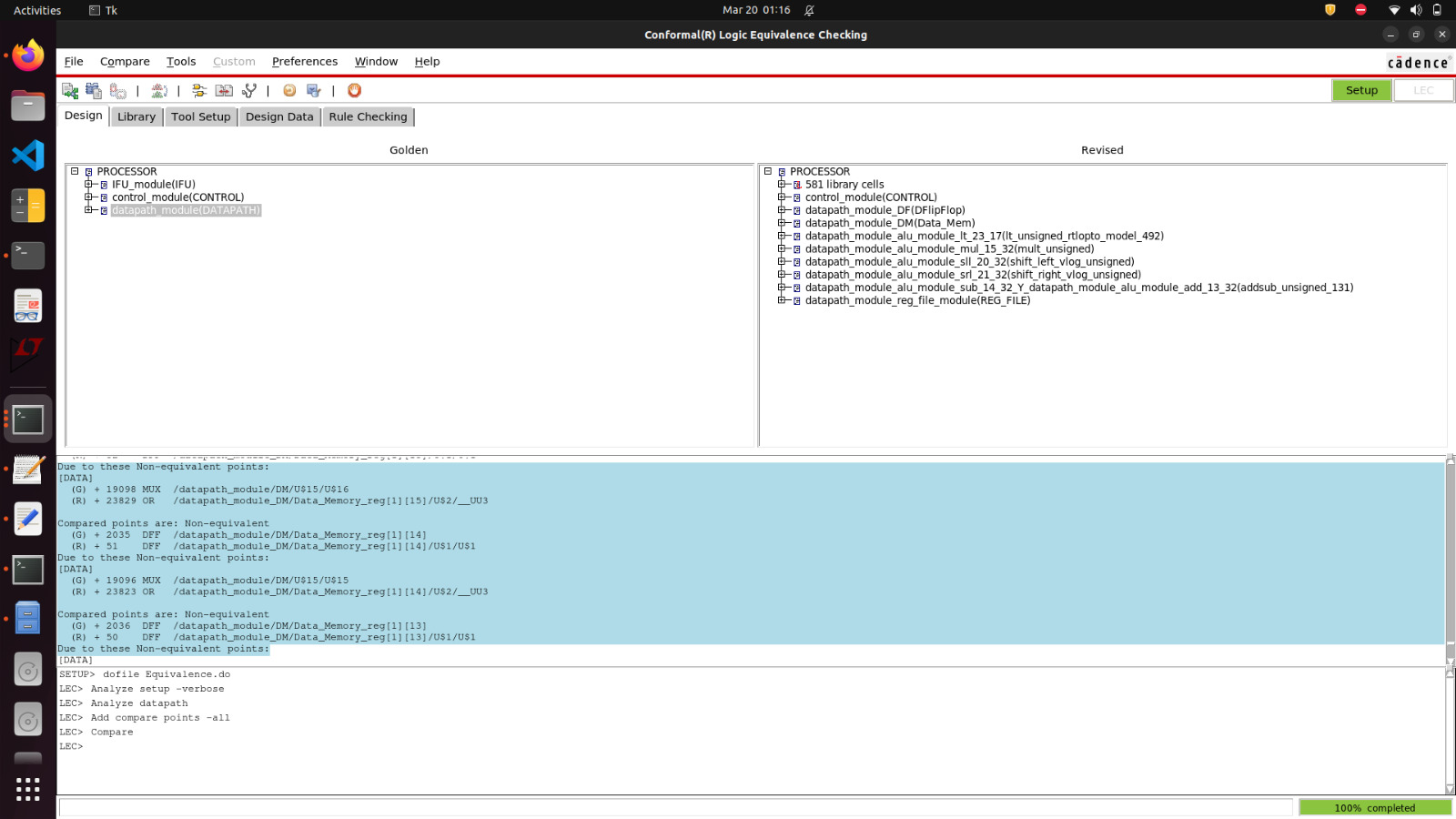
WHEN I COMPARING MY GOLDEN.V WITH revised netlist during conformal , I got these non-equivalent point for every reg memory and for every data memory. I don't know what to do with these non-equivalent point. I've been stuck here for the past four days. Please help me in this and how can I remove this non- equivalent point , since I am new to this I really don't know what to do.
WhatsApp Image 2024-03-20 at 1.17.02 AM.jpeg
WhatsApp Image 2024-03-20 at 1.17.27 AM.jpeg
 
I would start by chasing the latches. Why do you have so many?
Actually i create register file memory and data memory for my simple processor that's why they have so many there. You can look at my code below.


Code Verilog - [expand]
1
2
3
4
5
6
7
8
9
10
11
12
13
14
15
16
17
18
19
20
21
22
23
24
25
26
27
28
29
30
31
32
33
34
35
36
37
38
39
40
41
42
43
44
45
46
47
48
49
50
51
52
53
54
55
56
57
58
59
60
61
62
63
64
65
66
67
68
69
70
71
72
73
74
75
76
77
78
79
80
81
82
83
84
85
86
87
88
89
90
91
92
93
94
95
96
97
98
99
100
101
102
103
104
105
106
107
108
109
110
111
112
113
114
115
116
117
118
119
120
121
122
123
124
125
126
127
128
129
130
131
132
133
134
135
136
137
138
139
140
141
142
143
144
145
146
147
148
149
150
151
152
153
154
155
156
157
158
159
160
161
162
163
164
165
166
167
168
169
170
171
172
173
174
175
176
177
178
179
180
181
182
183
184
185
186
187
188
189
190
191
192
193
194
195
196
197
198
199
200
201
202
203
204
205
206
207
208
209
210
211
212
213
214
215
216
217
218
219
220
221
222
223
224
225
226
227
228
229
230
231
232
233
234
235
236
237
238
239
240
241
242
243
244
245
246
247
248
249
250
251
252
253
254
255
256
257
258
259
260
261
262
263
264
265
266
267
268
269
270
271
272
273
274
275
276
277
278
279
280
281
282
283
284
285
286
287
288
289
290
291
292
293
294
295
296
297
298
299
300
301
302
303
304
305
306
307
308
309
310
311
312
313
314
315
316
317
318
319
320
321
322
323
324
325
326
327
328
329
330
331
332
333
334
335
336
337
338
339
340
341
342
343
344
345
346
347
348
349
350
351
352
353
354
355
356
357
358
359
360
361
362
363
364
365
366
367
368
369
370
371
372
373
374
375
376
377
378
379
380
381
382
383
384
385
386
387
388
389
390
391
392
393
394
395
396
397
398
399
400
401
402
403
404
405
406
407
408
409
410
411
412
413
414
415
416
417
418
419
420
421
422
423
424
425
426
427
428
429
430
431
432
433
434
435
436
///////ALU
module ALU (
    input [31:0] A,B,
    input[3:0] alu_control,
    output reg [31:0] alu_result,
    output reg zero_flag
);
    always @(*)
    begin
        // Operating based on control input
        case(alu_control)
 
        4'b0001: alu_result = A+B;
        4'b0010: alu_result = A-B;
        4'b0011: alu_result = A*B;
        4'b0100: alu_result = A|B;
        4'b0101: alu_result = A&B;
        4'b0110: alu_result = A^B;
        4'b0111: alu_result = ~B;
        4'b1000: alu_result = A<<B;
        4'b1001: alu_result = A>>B;
        4'b1010: begin
            if(A<B)
            alu_result = 1;
            else
            alu_result = 0;
        end
        default: alu_result = A+B;
 
        endcase
 
        // Setting Zero_flag if ALU_result is zero
        if (alu_result)
            zero_flag = 1'b1;
        else
            zero_flag = 1'b0;  
    end
endmodule
 
 
/////CONTROL UNIT
/*
Control unit controls takes opcode, funct7, funct3 of the instruction code to determine
and control regwrite in IFU, alu control in ALU to execute proper instruction
*/
/*
Control unit controls takes opcode, funct7, funct3 of the instruction code to determine
and control regwrite in IFU, alu control in ALU to execute proper instruction
*/
module CONTROL(
    input [4:0] opcode,
    output reg [3:0] alu_control,
    output reg regwrite_control,memread_control,memwrite_control
);
    always @(opcode)
    begin
       case(opcode)
        5'b00001: begin alu_control=4'b0001;  //add
        regwrite_control=1; memread_control=0; memwrite_control=0;
        end
        5'b00010: begin alu_control=4'b0010;  ///sub
        regwrite_control=1; memread_control=0; memwrite_control=0;
        end
        5'b00011: begin alu_control=4'b0011;  //mul
        regwrite_control=0; memread_control=0; memwrite_control=1;
        end
        5'b00100: begin alu_control=4'b0100;  ///OR
        regwrite_control=0; memread_control=0; memwrite_control=1;
        end
        5'b00101: begin alu_control=4'b0101;  ///AND
        regwrite_control=1; memread_control=0; memwrite_control=0;
        end
        5'b00110: begin alu_control=4'b0110;  ///XOR
        regwrite_control=0; memread_control=0; memwrite_control=1;
        end
        5'b00111: begin alu_control=4'b0111;  ///NOT
        regwrite_control=0; memread_control=0; memwrite_control=1;
        end
        5'b01000: begin alu_control=4'b1000;  //SL
        regwrite_control=1; memread_control=1; memwrite_control=0;
        end
        5'b11001: begin alu_control=4'b1001;  //SR
        regwrite_control=1; memread_control=1; memwrite_control=0;
        end
        5'b01010: begin alu_control=4'b1010;  //COMPARE
        regwrite_control=1; memread_control=1; memwrite_control=0;
        end
        //5'b11010: begin ALU_control=4'b0000;  //SW
        //regwrite_control=1; memread_control=0; memwrite_control=0;
        //end
        //5'b01010: begin ALU_control=4'bxxxx;  //LW
        //regwrite_control=0; memread_control=0; memwrite_control=1;
        //end
        default : begin alu_control = 4'b0001;
        regwrite_control=1; memread_control=0; memwrite_control=0;
        end
        endcase 
    end
endmodule


//////DATA MEMORY
module Data_Mem(
input clock, rd_mem_enable, wr_mem_enable,
input [11:0] address,
input [31:0] datawrite_to_mem,
output reg [31:0] dataread_from_mem );
 
reg [31:0] Data_Memory[8:0];
 
initial begin
    Data_Memory[0] = 32'hFFFFFFFF;
    Data_Memory[1] = 32'h00000001;
    Data_Memory[2] = 32'h00000005;
    Data_Memory[3] = 32'h00000003;
    Data_Memory[4] = 32'h00000004;
    Data_Memory[5] = 32'h00000000;
    Data_Memory[6] = 32'hFFFFFFFF;
    Data_Memory[7] = 32'h00000000;
    //Data_Memory[8] = 32'h00000008;
    //Data_Memory[9] = 32'h00000009;
    //Data_Memory[10] = 32'h0000000A;
    //Data_Memory[11] = 32'h0000000B;
    //Data_Memory[12] = 32'h0000000C;
    //Data_Memory[13] = 32'h0000000D;
    //Data_Memory[14] = 32'h0000000E;
    //Data_Memory[15] = 32'h0000000F;
    //Data_Memory[16] = 32'h00000010;
    //Data_Memory[17] = 32'h00000011;
    //Data_Memory[18] = 32'h00000012;
    //Data_Memory[19] = 32'h00000013;
    //Data_Memory[20] = 32'h00000014;
    //Data_Memory[21] = 32'h00000015;
    //Data_Memory[22] = 32'h00000016;
    //Data_Memory[23] = 32'h00000017;
    //Data_Memory[24] = 32'h00000018;
    //Data_Memory[25] = 32'h00000019;
    //Data_Memory[26] = 32'h0000001A;
    //Data_Memory[27] = 32'h0000001B;
    //Data_Memory[28] = 32'h0000001C;
    //Data_Memory[29] = 32'h0000001D;
    //Data_Memory[30] = 32'h0000001E;
    Data_Memory[31] = 32'h0000001F;
      
    end
    always@(posedge clock) begin
       if(wr_mem_enable) begin
            Data_Memory[address] <= datawrite_to_mem;
       end
       else if(rd_mem_enable) begin
               dataread_from_mem <= Data_Memory[address];
       end
       else begin
               dataread_from_mem <= 32'h00000000;
       end
    end
endmodule  


/////INST MEM
/*
 
*/
module INST_MEM(
    input [31:0] PC,
    input reset,
    output [31:0] Instruction_Code
);
    reg [7:0] Memory [43:0]; // Byte addressable memory with 32 locations
 
   
    assign Instruction_Code = {Memory[PC+3],Memory[PC+2],Memory[PC+1],Memory[PC]};


    initial begin
            // Setting 32-bit instruction: add t1, s0,s1 => 0x00940333
            Memory[3] = 8'b0000_0000;
            Memory[2] = 8'b0000_0001;
            Memory[1] = 8'b0111_1100;
            Memory[0] = 8'b0000_0001;
            // Setting 32-bit instruction: sub t2, s2, s3 => 0x413903b3
            Memory[7] = 8'b0000_0000;
            Memory[6] = 8'b0000_0110;
            Memory[5] = 8'b1000_1111;
            Memory[4] = 8'b1110_0010;
            // Setting 32-bit instruction: mul t0, s4, s5 => 0x035a02b3
            Memory[11] = 8'b0000_0000;
            Memory[10] = 8'b0000_0101;
            Memory[9] = 8'b0111_1100;
            Memory[8] = 8'b0000_0011;
            // Setting 32-bit instruction: or t3, s6, s7 => 0x017b4e33
            Memory[15] = 8'b1111_1111;
            Memory[14] = 8'b1111_0100;
            Memory[13] = 8'b1010_0000;
            Memory[12] = 8'b1010_0100;
            // Setting 32-bit instruction: and
            Memory[19] = 8'b0000_0000;
            Memory[18] = 8'b0010_1001;
            Memory[17] = 8'b0001_1101;
            Memory[16] = 8'b0010_0101;
            // Setting 32-bit instruction: xor
            Memory[23] = 8'b0000_0000;
            Memory[22] = 8'b0001_1000;
            Memory[21] = 8'b0000_1101;
            Memory[20] = 8'b0110_0110;
            // Setting 32-bit instruction: not
            Memory[27] = 8'b0000_0000;
            Memory[26] = 8'b0010_1001;
            Memory[25] = 8'b0011_1101;
            Memory[24] = 8'b1100_0111;
            // Setting 32-bit instruction: shift left
            Memory[31] = 8'b0000_0000;
            Memory[30] = 8'b0101_0111;
            Memory[29] = 8'b1100_0110;
            Memory[28] = 8'b0000_1000;
            // Setting 32-bit instruction: shift right
            Memory[35] = 8'b0000_0000;
            Memory[34] = 8'b0110_1010;
            Memory[33] = 8'b1101_0010;
            Memory[32] = 8'b0111_1001;
            /// Setting 32-bit instruction: Campare
            Memory[39] = 8'b0000_0000;
            Memory[38] = 8'b0111_1010;
            Memory[37] = 8'b1101_0010;
            Memory[36] = 8'b0110_1010;
            /// Setting 32-bit instruction:
            Memory[43] = 8'b0000_0000;
            Memory[42] = 8'b0111_0111;
            Memory[41] = 8'b1101_0010;
            Memory[40] = 8'b0111_0010;
        end
  
 
endmodule
 
//IFU
/*
The instruction fetch unit has clock and reset pins as input and 32-bit instruction code as output.
Internally the block has Instruction Memory, Program Counter(P.C) and an adder to increment counter by 4,
on every positive clock edge.
*/
module IFU(
    input clock,reset,
    output [31:0] Instruction_Code
);
reg [31:0] PC = 32'b0;  // 32-bit program counter is initialized to zero
 
   
    always @(posedge clock, posedge reset)
    begin
        if(reset == 1)  //If reset is one, clear the program counter
        PC <= 0;
        else
        PC <= PC+4;   // Increment program counter on positive clock edge
    end
    // Initializing the instruction memory block
    INST_MEM instr_mem(.PC(PC),.reset(reset),.Instruction_Code(Instruction_Code));
 
endmodule
 
 
///MUX
 
module Mux_2X1 (
    input mem_rd_select, // rd_mem_enable
    input wire [31:0] dataread_from_mem, regdata2,
 
    output reg [31:0] mux_out
);
 
always @(mem_rd_select or dataread_from_mem or regdata2) begin
    if (mem_rd_select == 1)
        mux_out <= dataread_from_mem ;
    else
        mux_out <= regdata2;
    end
endmodule
 
//DFlipFlop
module DFlipFlop(D,clock,Q);
input D; // Data input
input clock; // clock input
output reg Q; // output Q
always @(posedge clock)
begin
 Q <= D;
end
endmodule
 
///DATA path
 
 
module DATAPATH(
    input [4:0]Read_reg_add1,
    input [4:0]Read_reg_add2,
    input [4:0]Reg_write_add,
    input [3:0]Alu_control,
    input [11:0]Address,
    input Wr_reg_enable,Wr_mem_enable,Rd_mem_enable,
    input clock,
    input reset,
    output OUTPUT
    );
 
    // Declaring internal wires that carry data
    wire zero_flag;
    wire [31:0]Dataread_from_mem;
    wire [31:0]read_data1;
    wire [31:0]read_data2;
    wire [31:0]Mux_out;
    wire [31:0]Alu_result;
    //wire [31:0]datawrite_to_reg;
 
    // Instantiating the register file
    REG_FILE reg_file_module(.reg_read_add1(Read_reg_add1),.reg_read_add2(Read_reg_add2),.reg_write_add(Reg_write_add),.datawrite_to_reg(Alu_result),.read_data1(read_data1),.read_data2(read_data2),.wr_reg_enable(Wr_reg_enable),.clock(clock),.reset(reset));
 
    // Instanting ALU
    ALU alu_module(.A(read_data1), .B(Mux_out), .alu_control(Alu_control), .alu_result(Alu_result), .zero_flag(zero_flag));
   
    //Mux
    Mux_2X1 mux(.mem_rd_select(Rd_mem_enable),.dataread_from_mem(Dataread_from_mem),.regdata2(read_data2),.mux_out(Mux_out));
 
    //Data Memory
    Data_Mem DM(.clock(clock),.rd_mem_enable(Rd_mem_enable),.wr_mem_enable(Wr_mem_enable),.address(Address),.datawrite_to_mem(Alu_result),.dataread_from_mem(Dataread_from_mem));
   
    // Dflipflop
    DFlipFlop DF (.D(zero_flag), .Q(OUTPUT),.clock(clock));
endmodule
 
 
/*
A register file can read two registers and write in to one register.
The RISC V register file contains total of 32 registers each of size 32-bit.
Hence 5-bits are used to specify the register numbers that are to be read or written.
*/
 
/*
Register Read: Register file always outputs the contents of the register corresponding to read register numbers specified.
Reading a register is not dependent on any other signals.
 
Register Write: Register writes are controlled by a control signal RegWrite. 
Additionally the register file has a clock signal.
The write should happen if RegWrite signal is made 1 and if there is positive edge of clock.
*/
module REG_FILE(
    input [4:0] reg_read_add1,
    input [4:0] reg_read_add2,
    input [4:0] reg_write_add,
    input [31:0] datawrite_to_reg,
    output [31:0] read_data1,
    output [31:0] read_data2,
    input wr_reg_enable,
    input clock,
    input reset
);
 
    reg [31:0] reg_memory [31:0]; // 32 memory locations each 32 bits wide
   
    initial begin
        reg_memory[0] = 32'h00000000;
        reg_memory[1] = 32'hFFFFFFFF;
        reg_memory[2] = 32'h00000002;
        reg_memory[3] = 32'hFFFFFFFF;
        reg_memory[4] = 32'h00000004;
        reg_memory[5] = 32'h01010101;
        reg_memory[6] = 32'h00000006;
        reg_memory[7] = 32'h00000000;
        reg_memory[8] = 32'h10101010;
        reg_memory[9] = 32'h00000009;
        reg_memory[10] = 32'h0000000A;
        reg_memory[11] = 32'h0000000B;
        reg_memory[12] = 32'h0000000C;
        reg_memory[13] = 32'h0000000D;
        reg_memory[14] = 32'h0000000E;
        reg_memory[15] = 32'h0000000F;
        reg_memory[16] = 32'h00000010;
        reg_memory[17] = 32'h00000011;
        reg_memory[18] = 32'h00000012;
        reg_memory[19] = 32'h00000013;
        reg_memory[20] = 32'h00000014;
        reg_memory[21] = 32'h00000015;
        //reg_memory[22] = 32'h00000016;
        //reg_memory[23] = 32'h00000017;
        //reg_memory[24] = 32'h00000018;
        //reg_memory[25] = 32'h00000019;
        //reg_memory[26] = 32'h0000001A;
        //reg_memory[27] = 32'h0000001B;
        //reg_memory[28] = 32'h0000001C;
        //reg_memory[29] = 32'h0000001D;
        //reg_memory[30] = 32'h0000001E;
        reg_memory[31] = 32'hFFFFFFFF;
    end
 
    // The register file will always output the vaules corresponding to read register numbers
    // It is independent of any other signal
    assign read_data1 = reg_memory[reg_read_add1];
    assign read_data2 = reg_memory[reg_read_add2];
 
    // If clock edge is positive and regwrite is 1, we write data to specified register
    always @(posedge clock)
    begin
        if (wr_reg_enable) begin
            reg_memory[reg_write_add] = datawrite_to_reg;
        end    
    else
        reg_memory[reg_write_add] = 32'h00000000;
    end
endmodule
 
 
/////PROCESSOR
 
 
module PROCESSOR(
    input clock,
    input reset,
    output Output
);
 
    wire [31:0] instruction_Code;
    wire [3:0] ALu_control;
    wire WR_reg_enable;
    wire WR_mem_enable;
    wire RD_mem_enable;
 
 
    IFU IFU_module(.clock(clock), .reset(reset), .Instruction_Code(instruction_Code));
   
    CONTROL control_module(.opcode(instruction_Code[4:0]),.alu_control(ALu_control),.regwrite_control(WR_reg_enable),.memread_control(RD_mem_enable),.memwrite_control(WR_mem_enable));
   
    DATAPATH datapath_module(.Wr_mem_enable(WR_mem_enable),.Rd_mem_enable(RD_mem_enable),.Read_reg_add1(instruction_Code[9:5]),.Read_reg_add2(instruction_Code[14:10]),.Reg_write_add(instruction_Code[19:15]),.Address(instruction_Code[31:20]),.Alu_control(ALu_control),.Wr_reg_enable(WR_reg_enable), .clock(clock), .reset(reset), .OUTPUT(Output));
 
endmodule

 
Last edited by a moderator:
I am not entirely sure and can't simulate/eval your code, but likely the issue is how you coded the instruction memory content as initial statements.


LaTeX Commands Quick-Menu:

Similar threads

Part and Inventory Search

Welcome to EDABoard.com

Sponsor

Back
Top