Continue to Site

Welcome to EDAboard.com

Welcome to our site! EDAboard.com is an international Electronics Discussion Forum focused on EDA software, circuits, schematics, books, theory, papers, asic, pld, 8051, DSP, Network, RF, Analog Design, PCB, Service Manuals... and a whole lot more! To participate you need to register. Registration is free. Click here to register now.

Compensating a 3 gate 4069 amplifier

Status
Not open for further replies.

Eugen_E

Full Member level 6
Full Member level 6
Joined
Nov 29, 2004
Messages
387
Helped
44
Reputation
86
Reaction score
11
Trophy points
1,298
Location
Romania
Activity points
2,878
Hello,
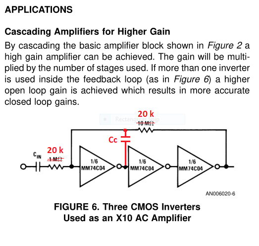
I've tried to use in a circuit this improved (high gain, 3 gates) 4069 amplifier from the old AN-88 (National Semiconductor),
instead of a better amplifier, because I had unused gates available.
This is used at very low frequency and DC, so low bandwidth is not a problem.
I built the circuit with 20 k resistors (values in red), VDD=5 V, and it oscillates at about 2.4 MHz.
4069_3gates.PNG


Then I tried to compensate the amplifier by adding Cc:
  • for Cc = 22 nF, it oscillates at about 38 kHz
  • for Cc = 100 nF, it oscillates at about 9.8 kHz.
Is it possible to compensate this amplifier, keeping the resistor values to 20 k and how to do it?
Should I use a proper opamp amplifier?

Thanks
 
Last edited:

Solution
Your result supports my conclusion, that the three inverter circuits isn't unconditionally stable. I presume you are using the same CD4069 model by Helmut Sennewald. If so, the difference between post #15 and #16 is probably in selection of the SPICE integration method. I'm using Gear instead of default modified trap. Hard to say which setting better fits the real hardware behaviour.
--- Updated ---

I see that reducing the maximum timestep in transient analysis (=increasing simulation accuracy) makes the circuit also unstable. Thus we can conclude that this CD4049 model is actually unstable with 1M/10M feedback resistors and 9V supply.
--- Updated ---

I was finally able to make the circuit stable by using lag-lead compensation...
There's probably a very good reason National specified the resistors that they did. You want a unity-gain amplifier; they've got a X10 amplifier. Sometimes amplifiers are not stable at unity gain. If you really want to use this method then I suggest you use the resistors National recommends and then put a voltage divider on the output.
 

Hi,
Should I use a proper opamp amplifier?
This probably is what I would do.

But without knowing what it has to drive...
We have no idea about voltage, current, frequency range, waveform, accuracy, noise, distortion...

Klaus
 

A few points to consider:
1. The original AN-88 circuit is using unbuffered (single inverter) gates, CD4069 is a buffered (three inverter) gate which much higher gain in linear range.
2. It's not claimed in AN-88 that the suggested circuit is stable under all possible conditions, e.g. unity gain.
3. It has to be carefully analyzed if the tested compensation circuit actually creates stability.

Please clarify if you are using CD4069 or CD4069U.
 

    Eugen_E

    Points: 2
    Helpful Answer Positive Rating
Only the 'U' (unbuffered) version will work. The 74C04 shown in your schematic will not work. I would expect 'Cc' to be omitted or a very small value, only a few pF.

Brian.
 

    Eugen_E

    Points: 2
    Helpful Answer Positive Rating
Here is AN-88 (most of it) showing the 74C04 used as amp.

Attached.

In general as previously stated by several members an OpAmp much better
choice for amplifying, either a V OpAmp or a Current (Norton) OpAmp, as
they are much better characterized for amp applications, and CMOS totem
pole inverters draw a lot of current when in linear region.

I cannot find a buffered datasheet of the CD4069, looking because I think,
but not sure, its buffered by paralleling more fets on output not series
them. To increase output current capability.


Regards, Dana.
 

Attachments

  • AN-88.pdf
    2.3 MB · Views: 241
Last edited:

    Eugen_E

    Points: 2
    Helpful Answer Positive Rating
Thanks for the replies, I'm using an CD4069UBE, from TI - it is unbuffered.
I searched for schematics of analog applications for 4069. It seems nowadays is used a lot for guitar effects, and all schematics use only one inverter per stage (but this is maybe to get the distorsion needed).

I'll try to use higher value resistors (100k ... 1 Meg), maybe 20 k is too low for unbuffered CMOS. I expected it to be stable even with the input not connected.

PS. In AN-88, circuits in figures 7, 8, 9 are interesting - post opamp amplifiers, even with 2 gates, still stable at very high open loop gain. Figure 7, 9 are even unity gain.
 
Last edited:

Keep in mind using these inverters as G elements ignores some pretty important
design consideration such as CMR and PSRR. PSRR especially will couple
directly into signal chain, so if your supply rail has a couple hundred mV of
trash on it you will see virtually no rejection to that. Pay attention to caps you use to
bypass, as you can see below for the same capacitance a wide variation in bypass
performance due to ESR differences.

1636129963159.png


Regards, Dana.
 

I wonder if the three inverter circuit has been verified by the AN-88 author(s). I wasn't yet able to find a stable dimensioning in LTSpice simulation.
 

Forrest Mims has the 3-gate 4049 schematic in his Engineer's Notebook pg 20 ('linear 10X amplifier'). Resistor values are 1M & 10M similar to post #1 schematic.
I built a mic pre-amp with 4069UBE (unbuffered) and it works very well from battery power.

In 'Getting started in electronics' pg 119 Mims has a two-input NAND gate (4011 IC) functioning as a 'linear x10 amplifier' (calling it a 'non-digital role for a digital gate'). Only one stage is used. Resistor values 1M & 10M.

These books contain sections about 7400 series IC's but I find none showing a similar analog-style amplifier made from digital gates.

It appears that 7400 series do not work as easily in this non-digital role. I'm testing various 7404 IC's as a plain invert-gate.

1) First I leave input unconnected. Output is low by default, and stable even though input is floating.

2) Then I apply 0V through 10k potentiometer to the input. Output remains low.

3) I dial resistance down to a few K. Then output goes high.
Output rises or falls as I alter resistance. Output does not snap quickly to a high or low supply rail.
This behavior makes it seem as if the input has an internal pull-up resistor.

My IC's are 40 or 50 yrs old but I don't see that it should severely affect behavior.
 
Last edited:

using gates as a x10 amp is a bad idea unless the input is tightly conditioned in terms of amplitude and freq range.
 

Hi

AN-88 is from 1973 .. almost 50 years back.
About 5 years after LM741 was designed, times without internet, without good available datasheets and application note, without a big variety of Opams ...
One had to use the semiconductors that were available.
Times have changed.
I'd rather use an Opamp from an old PCB than doing handstands with a device not designed for this use case. With in best case mediocre ... maybe even unreliable results.

Klaus
 
Brad, the original design specified a CD4069U which was a rather unusual digital inverter because it simply used two mosfets. It was possible to apply feedback from output to input to bias both devices into conduction simultanously so its output sat at about half supply voltage and it had a reasonably linear transfer characteristic. Later versions, without the 'U' behaved more like conventional logic inverters. To the best of my knowledge that was the only digital device except some ECL ICs that could be used that way and certainly none of the 74 series would work.

Brian.
 
I could finally verify stable operation of the AN-88 three inverter circuit with LTspice, using the CD4069U model published by Helmut Sennewald at https://groups.io/g/LTspice

At least with this model, the circuit is not stable at 5V supply voltage, but it might be in real hardware due to different transistor threshold voltage.

While the single inverter amplifier is unconditionally stable independent of feedback resistors and supply voltage, the three inverter circuit obviously isn't. You need to analyze the loop gain to determine stability.

As stated by danadakk in post #7, all CD4069 available on the market are unbuffered CD4069U types, in contrast e.g. to 74HC04 which is generally buffered except for dedicated unbuffered 74HC04U.

1636278058293.png
 

Attachments

  • CD4069U_amp.zip
    1.6 KB · Views: 163
Last edited:
I tried the simulation posted above in LTSpice XVII.
It still oscillates, even with a 9 V supply, with different resistor values, etc. . The startup transient is obvious.
4069_oscillating.PNG

CD4069 has a guaranteed input current lower than 1 pA, in DIP package, this would be the only advantage for my circuit.
 

Your result supports my conclusion, that the three inverter circuits isn't unconditionally stable. I presume you are using the same CD4069 model by Helmut Sennewald. If so, the difference between post #15 and #16 is probably in selection of the SPICE integration method. I'm using Gear instead of default modified trap. Hard to say which setting better fits the real hardware behaviour.
--- Updated ---

I see that reducing the maximum timestep in transient analysis (=increasing simulation accuracy) makes the circuit also unstable. Thus we can conclude that this CD4049 model is actually unstable with 1M/10M feedback resistors and 9V supply.
--- Updated ---

I was finally able to make the circuit stable by using lag-lead compensation. Phase margin is rather low, just want to show that it's basically possible. You can plot loop gain as V(o)/V(i).

1636797343959.png
 
Last edited:
Solution
...the difference between post #15 and #16 is probably in selection of the SPICE integration method. I'm using Gear instead of default modified trap. Hard to say which setting better fits the real hardware behaviour.
Which is why you ultimately need to actually go into the lab and test some real hardware.
 
  • Like
Reactions: FvM

Hello,
I've tried to use in a circuit this improved (high gain, 3 gates) 4069 amplifier from the old AN-88 (National Semiconductor),
instead of a better amplifier, because I had unused gates available.
This is used at very low frequency and DC, so low bandwidth is not a problem.
I built the circuit with 20 k resistors (values in red), VDD=5 V, and it oscillates at about 2.4 MHz.

View attachment 172706

Then I tried to compensate the amplifier by adding Cc:
  • for Cc = 22 nF, it oscillates at about 38 kHz
  • for Cc = 100 nF, it oscillates at about 9.8 kHz.
Is it possible to compensate this amplifier, keeping the resistor values to 20 k and how to do it?
Should I use a proper opamp amplifier?

Thanks
If you remove Cc, your circuit behaves as an opamp with gain=-1. Cc introduces a positive feedback around 2nd-3rd stage making it an oscillator. As you are using it at low frequency, my suggestion is to go back to the original values, remove Cc, and remove the second and third HC04. A single stage can easly provide the gain of 10. If you don't have 1M/10M resistors, try to reduce their values, but keep the x10 ratio between the two. I would not go below 1M for the second resistor for two reasons: to avoid loading the output stage, but most important, as the gates have an input capacitance Cgate that can make the circuit oscillate if R x Cgate is too small. Having R larger, makes the loop gain small avoiding oscillations.
A curiosity: once, I made a 80MHz oscillator out of a HC04 (regular one) using a 16MHz Xtal in 5th overtone. It got a bit hot but oscillated quite nicely and stable, providing a low power FM broadcast station. CMOS can go a long way.
Last suggestion: always try to put reference next to components (e.g. R1, R2, C1, etc.), as it makes discussion less ambiguous :).
 

Status
Not open for further replies.

Similar threads

Part and Inventory Search

Welcome to EDABoard.com

Sponsor

Back
Top