Continue to Site

Welcome to EDAboard.com

Welcome to our site! EDAboard.com is an international Electronics Discussion Forum focused on EDA software, circuits, schematics, books, theory, papers, asic, pld, 8051, DSP, Network, RF, Analog Design, PCB, Service Manuals... and a whole lot more! To participate you need to register. Registration is free. Click here to register now.

coin-cell battery footprint problem

Status
Not open for further replies.

Kick

Full Member level 6
Full Member level 6
Joined
Sep 27, 2010
Messages
345
Helped
16
Reputation
32
Reaction score
15
Trophy points
1,298
Location
India,Bangalore
Activity points
3,178
hiii all,

In my circuit there is a coin-cell battery and I placed bottom side of the board,some vias also present in the battery footprint area.My doubt is when i m inserting battery in battery holder will it contact with vias and circuit become short???
 

It depends on how the board was made. Some vias are tented (covered with mask) that protects them from being contacted and encapsulates them. I would check if this was the case. You could also do a continuity check on the via if you have access to it.
 

You cannot rely on solder mask as an insulator, if anything goes wrong you could be liable, if this is a commercial product. if it is for yourself you have to think of the possible downsides a short may cause.
Even if it does insulate initially, the resist can be easily worn of pads, either design it so there will be no shorts or use a proper insulating material.
 

when i m inserting battery in battery holder will it contact with vias and circuit become short???

I can´t see how this could happen if you use a standard holder like that.
Note the bottom surface insulates completely the battery from PCB board.

2293258-40.jpg
 

I am using SMD type battery holder.
 

Attachments

  • bat holder.jpg
    bat holder.jpg
    29.1 KB · Views: 132

Dear Kick,
From the picture, i hope the battery will be placed directly on the pcb and the holder will be fixed on top of it. Is that right?
If so, the pcb will be having a pad of the size of the battery for the negative terminal. Then how can you have any other vias in that area??
 

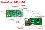
yup..u r right..in my board there is 10mm dia pad for -ve terminal.But i saw same battery bolder in another circuit,they used small size pad for -ve terminal and also i saw vias around that pad.

- - - Updated - - -

In this pic u can see vias around -ve terminal
 

Attachments

  • z3.jpg
    z3.jpg
    113 KB · Views: 116

Tented vias provides insulation.But still this is 'very risky, as i see.
 
  • Like
Reactions: Kick

    Kick

    Points: 2
    Helpful Answer Positive Rating
Status
Not open for further replies.

Part and Inventory Search

Welcome to EDABoard.com

Sponsor

Back
Top