Continue to Site

Welcome to EDAboard.com

Welcome to our site! EDAboard.com is an international Electronics Discussion Forum focused on EDA software, circuits, schematics, books, theory, papers, asic, pld, 8051, DSP, Network, RF, Analog Design, PCB, Service Manuals... and a whole lot more! To participate you need to register. Registration is free. Click here to register now.

Clock requirements from manual regrding dac80004

Status
Not open for further replies.

yefj

Advanced Member level 5
Joined
Sep 12, 2019
Messages
1,505
Helped
1
Reputation
2
Reaction score
5
Trophy points
38
Activity points
9,113
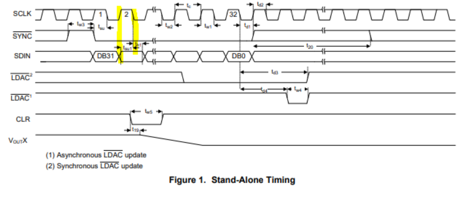
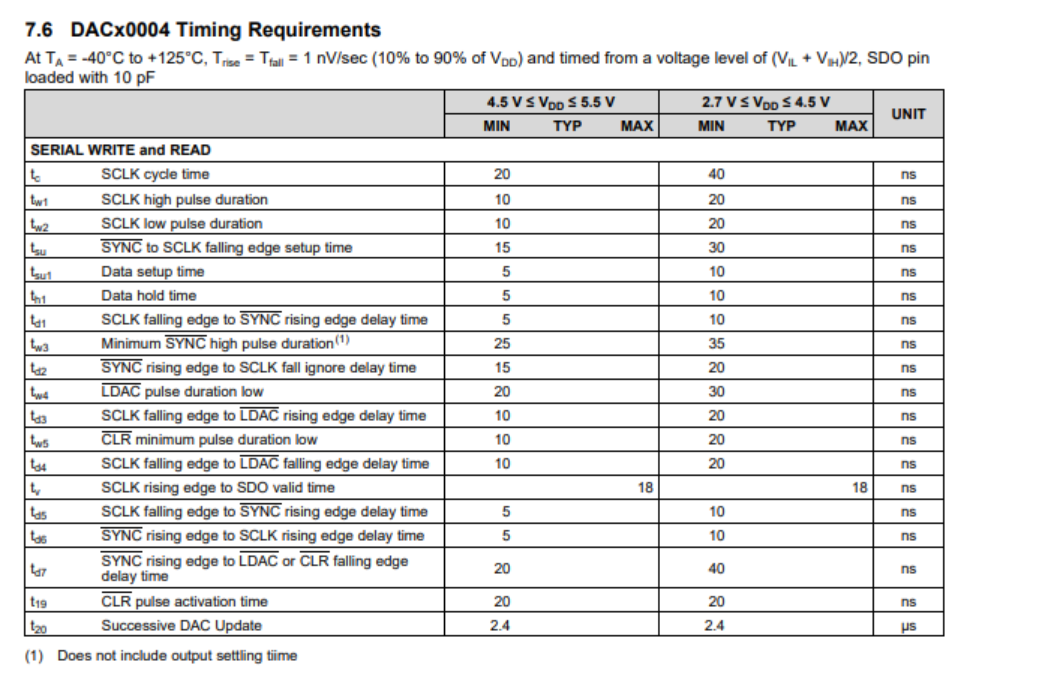
Hello ,In the datasheet shown bellow we have a table of timing requirements.
I cant see from the table and from the diagram bellow why i should complute my SPI with sampling in FALLING EDGE?
if you could please draw the arrrow up and down on the diagram so i understand why they want a falling edge samplin?
because as i can see the clock could be both on rising and falling in this place.
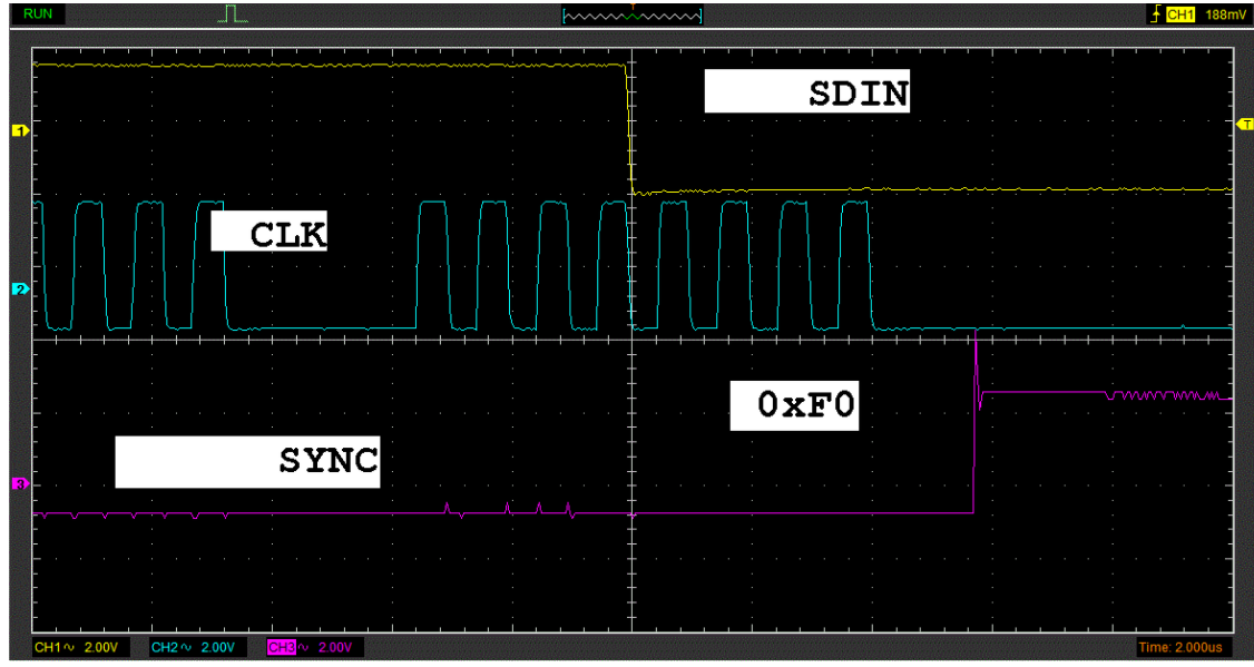
In the photo shown bellow there is a photo of my SPI sequence,How can i see visualy that it sampling or rising edge?
Thanks.
1601570465099.png

1601570553852.png


1601571595805.png
 
Last edited:

Hi,

as you can see, for a falling edge the data input SDIN provides a stable/steady value. Whereas, if sampled/clocked-in on a rising edge SDIN is in transition (high-t-o low or low-to-high) and no steady value (except for a consecutive HIGHs or LOWs) can be ensured.

You have to set the clock-polarity and phase of the SPI bus (microcontroller as a master) correct. Have a look at [1].

[1] https://en.wikipedia.org/wiki/Serial_Peripheral_Interface

BR
--- Updated ---

You might be lucky and the data value is in a steady state for the rising edge, but you have to consider parastic capacitances caused by the PCB layout as well as the input capacitances of other ICs attached to the SPI bus. Thus a longer time is required to charge and discharge those capacitances and consequently to reach the correct/steady value.

BR
 

Yes but i cant see from my diagram nor in the diagram in the manual that they want falling edge and i have rissing edge(not by looking at the code)
i am having problem to interpret it visually.
Thanks.
 

Ok, the oscilloscope graph wasn't visible for me before.

According to your scope graph, you have configured the MCU with CPOL=0 and CPHA=0.
According to the image attached by you, taken from the datasheet the following configuration should be used: CPOL=0 and CPHA=1.

nor in the diagram in the manual that they want falling edge

Have a look at section 8.4, there the falling edge is mentioned several times.

BR
 

Hello.

"sampling" of SPI data means "latching the input" on the receiving device. In your case the DAC.
So the master (microcontroller) outputs it´s data on MOSI at the rising clock edge, while the DAC samples the data on the falling edge.

if you connect SO of the DAC to MISO of your microcontroller (not necessary), then:
The DAC outputs it´s data on MISO at the rising clock edge, while the microcontroller samples the data on the falling edge.

Klaus
 

Hi,

So the master (microcontroller) outputs it´s data on MOSI at the rising clock edge, while the DAC samples the data on the falling edge.

as you can see in your attached scope image, the microcontroller changes its output state at the falling clock edge, which causes troubles as the DAC latches the SDIN value (which is the data provided by the MCU) in, when the clock changes from high to low.

BR
 

Yes but i cant see from my diagram nor in the diagram in the manual that they want falling edge and i have rissing edge(not by looking at the code)
i am having problem to interpret it visually.
It's very clearly stated in the diagram by specification of setup and hold time tsu and th. Both are referring to the active, in this case falling edge.
 

Hello ,How do you see it fromt he photo,can i have some visual rule of thumb to recognise it?
I cant see where is the rising or falling edge on my clock photo of the scope.COuld you please put an arrows on the photo bellow.
Thanks.

Ok, the oscilloscope graph wasn't visible for me before.

According to your scope graph, you have configured the MCU with CPOL=0 and CPHA=0.
According to the image attached by you, taken from the datasheet the following configuration should be used: CPOL=0 and CPHA=1.


Have a look at section 8.4, there the falling edge is mentioned several times.

BR

1601722813335.png
 
Last edited:

IMG_20201003_140731.png


In the attached image the rising edge is marked.

Keep in mind, the time base of the scope starts on the left and ends on the right.

BR
 

In your waveform, SDIN is changing state at the falling clock edge, but the datasheet expects it to be set at the rising edge. Wrong clock polarity in the SPI setup.
 

Status
Not open for further replies.

Similar threads

Part and Inventory Search

Welcome to EDABoard.com

Sponsor

Back
Top