kender
Advanced Member level 4

OrCAD. Clearance between copper pour and board outline
Folks,
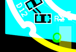
I’m laying out a PCB with an intricate outline. First, I drew the outline (yellow in the picture below). Then I’ve added a copper pour at the top layer (blue in the picture below), but a clearance between the outline and the pour wasn’t created. The board outline didn’t clip the copper pour. (The clearance between copper pour and traces, components was created as expected.)
How can I enable clearance between copper pour and board outline?
Any suggestion, insight or reference is really appreciated!
Best,
- Nick
Folks,
I’m laying out a PCB with an intricate outline. First, I drew the outline (yellow in the picture below). Then I’ve added a copper pour at the top layer (blue in the picture below), but a clearance between the outline and the pour wasn’t created. The board outline didn’t clip the copper pour. (The clearance between copper pour and traces, components was created as expected.)
How can I enable clearance between copper pour and board outline?
Details for the board outline.
Obstacle type: Board Outline. Layer: Global Layer. Width: 40 mils.
Details for copper pour:
Obatscle type: Copper Pour. Layer: Top. Width:10. Clearance: 10
I’m on OrCAD 10.5
Obstacle type: Board Outline. Layer: Global Layer. Width: 40 mils.
Details for copper pour:
Obatscle type: Copper Pour. Layer: Top. Width:10. Clearance: 10
I’m on OrCAD 10.5
Any suggestion, insight or reference is really appreciated!
Best,
- Nick
