Continue to Site

Welcome to EDAboard.com

Welcome to our site! EDAboard.com is an international Electronics Discussion Forum focused on EDA software, circuits, schematics, books, theory, papers, asic, pld, 8051, DSP, Network, RF, Analog Design, PCB, Service Manuals... and a whole lot more! To participate you need to register. Registration is free. Click here to register now.

Circuit with an integrated FLIP FLOP

Status
Not open for further replies.

tnnedaboard

Member level 3
Member level 3
Joined
Apr 5, 2012
Messages
64
Helped
0
Reputation
0
Reaction score
0
Trophy points
1,286
Activity points
1,748
Hello everyone,

I have to make a small circuit with an integrated FLIP FLOP that has this function:

1. pin A and B input to 1, pin C output goes to 1
2. when pin A is 1 and pin B is 0, pin C goes to 0 and remains there even if pin B returns to 1
3. pin C returns to 1 only when pin A goes from 1 to 0 and then to 1 again and with pin B to 1

how could I do? Help thanks.
 

This is a mess.

In "1." you say C goes to 1 when A and B are 1. Then in "3." you say "pin C returns to 1 ONLY when pin A goes from 1 to 0 and then to 1 again and with pin B to 1". These two statements are contradictory. Maybe you should draw a timing diagram; that would help you and us.
 

Hi,

can you please draw a truth table,

your 1) violates your 2)
--> I assume: when pinA = 1 and pinB = 1: do nothing = hold mode = no change

your 2) is O.K.

your 3) reduces to: when pinA goes from 0 to 1 while pinB = 1: ouput = 1


****
What happens when pinB = 0 while pinA goes from 0 to 1?

Klaus

- - - Updated - - -

Hi,

my first approach:

DFF with asynchronous Reset:

D = pinB
Clk = pinA
Rst = /pinB
Q = output


Klaus
 

Can you give me an example of circuit …

At power on, C goes to 1 if A and B are at 1.
After if B goes from 1 to 0, C goes to 0 and stays there until there is a reset of the circuit….

I hope this is clearer …

Immagine1.jpg
 
Last edited:

Could I kindly have an example of a circuit to start from?

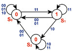
this is the state diagram

Immagine3.jpg
 

Hi,

"my first approach" of post#3 should give all you need to know.

If not, then do an internet search with the given informations.

Klaus
 

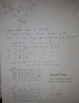
From the state diagram you can sythesize a sequential network. Since each FF can store 2 states, but you have 3 states you will need 2 FF. I started the derivation, I think you can continue by yourself adding the network that produces the wanted output for each state and finally drawing the schematic.

FlipFlop.jpg

Please check that I didn't make some error in placing the number into the state table or the K-maps
 

From the state diagram you can sythesize a sequential network. Since each FF can store 2 states, but you have 3 states you will need 2 FF. I started the derivation, I think you can continue by yourself adding the network that produces the wanted output for each state and finally drawing the schematic.

View attachment 158526

Please check that I didn't make some error in placing the number into the state table or the K-maps

Kindly, can you complete the states table?

the integrated CD74HC74, could it be fine? https://www.ti.com/lit/ds/symlink/cd74hc74.pdf
 

Yes, you can use the FF CD74HC74.
I don't think is correct I do the homeworks for you. I just gave you an hint on how to proceed (an plese check the figures I used are correct). Anyway to generate the output you want (that is the level related to each state) you have to synthesize a logic that involves Q0 and Q1 (outputs of the two FFs)
 

Yes, you can use the FF CD74HC74.
I don't think is correct I do the homeworks for you
I absolutely don't want this ...

However, in the meantime, it made it simpler, that is, with the evergreen NE555 and two transistors ...

What do you think?

schema.jpg
 

I didn't analyze in detail the circuit with 555, in any case it isn't a state machine. Using FF (the synchronous in and out) you'll have the change among states (then the outputs) synchronized with an incoming clock. What exactly have you been asked to design ?
 

Hi,

Interesting circuit implementation of the idea.

I noticed T = 1 x R x C. It's actually T = 1.1 x R x C for the 555 monostable. 2 x 4.7uF in parallel and 100k = 1.034 seconds. The trigger capacitor could be much smaller, but so long as trigger is shorter than pin 3 high duration your trigger RC is fine.

Walt Jung's IC Timer Cookbook pdf is easy to get on the Internet and has some 555 flipflops and so on you might want to copy or adapt to your needs.

Maybe an AND gate for A and B into a CD4017 clk pin and output 2 or 3 into reset could achieve the goal. Or using clk, !clk and reset of the 4017.

I may not have understood how your circuit works. Are SW A and SW B pushbuttons or signals? I ask as I did a little truth table for the circuit and it looks like C, the NPN, is always on in every of the four conditions you have, so the relay coil is energized in both POR conditions and in both "after x minutes" conditions. Maybe I misunderstood something about the circuit operation. Have you tested to see if it works?
 

Hi,

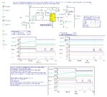
Had time to think about the circuit requiement. Here is an alternate version that also uses a monostable 555 annd BJTs. I hope I understood the function and this achieves it.

555 ABC POR CIRCUIT.JPG

- - - Updated - - -

Whoops, your version also uses two BJTs, not three, my mistake, couldn't fully remember the schematic. :)

Anyway, hope your question is solved with one circuit or another or the ff suggested version.
 

Status
Not open for further replies.

Part and Inventory Search

Welcome to EDABoard.com

Sponsor

Back
Top